IT-5-P-2506 Dynamic, Analytical EDX studies of B/Ni composite nanowires with MEMS heating holder
EDX measurements at high temperatures were a challenge for many years due to the technology constrains of the past related to the limitations of commercial Si(Li) EDX (energy-dispersive X-ray spectroscopy) detectors. With a newly designed MEMS holder and state-of-the-art SDD technology nowadays analytical EDX studies at elevated temperatures can be performed on a regular basis in a Scanning Transmission Electron Microscope (S/TEM), FEI’s TalosTM with ChemiSTEMTM Technology [1].
Here we present fast chemical maps of B/Ni composite nanowires on nanometer scale by EDX which were done with the new VeloxTM software, see Figure 1. Successful synthesis of crystalline nanowires composed of the refractory light materials such as Boron can enable novel applications for nanoelectronics [2-5]. Boron/Nickel composite nanostructures were prepared by a CVD-based synthetic procedure with a Ni-based compound catalyst; naturally blended with high conductivity and refraction index. The properties of this binary nanomaterial at room temperature, Figure 2, are compared to those achieved from heating experiments with temperatures up to 1000 °C. 2D-3D EDX chemical mappings show clearly the core-shell structure of the wires: B in the shell and Ni in the core. This is amplified at elevated temperatures of ca. 500 °C, see Figure 3. At ca. 1,000 °C EDX maps reveal also that Ni vanishes from the core, leaving behind hollow B nanowire (nanotube) structures.
For the given in situ experiments FEI’s NanoExTM heating holder was used with a small, consumable semiconductor (MEMS) device as the heater and providing a direct read-out of the temperature value at all times during the dynamic experiment with a known and reproducible temperature distribution over the heated area. The NanoEx solution is optimized for ChemiSTEM EDX experiments to trace compositional changes correlated with temperature and electrical stimuli. The holder geometry is suitable for high tilt angles, also allowing its use for 3D experiments.
[1] P. Schlossmacher et al., Microscopy Today 18(4) (2010) 14.
[2] CJ Otten, et al., J Am Chem Soc. 2002 May 1;124(17):4564.
[3] D. Wang et al., APL 2003, 183(25):5280.
[4] W. Ding et al., Mech, Comp. Sci. and Techn. 2006, 66:1109.
[5] J. Tian, et al., “Boron nanowires for flexible electronics”,APL 2008 93:122105-7-5.
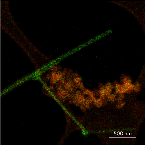
Fig. 1: EDX compositional maps of Boron nanowires at room temperature. The total acquisition time is ca. 10 minutes for the map sized 256 x 256 Px with a speed of 9.1 ms/Px and ~50cs/Px signal for the B-K edge. |
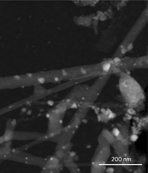
Fig. 2: Dynamic EDX compositional analysis at the begin of the experiment at room temperature. |
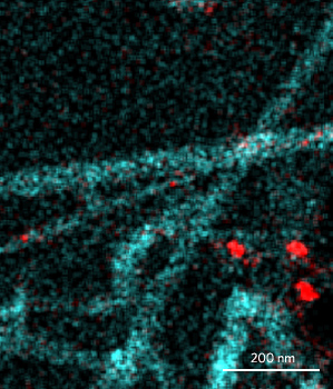
Fig. 3: Dynamic EDX compositional analysis comparing the same area at the heating temperature of 500 °C showing the Ni particles before they disappear when the heating temperature gets further raised and the specimen finally got cooled down. |
|