IT-2-IN-2458 Advanced scanning transmission electron microscopy with segmented annular all field detector
In this talk, I will review our recent and on-going findings from our exploration of new atomic-resolution imaging modes using an area detector which is capable of atomic-resolution STEM imaging [1]. One possibility is atomic-resolution differential phase contrast (DPC) imaging [2]. It has been reported that, to a good approximation, DPC STEM images represent the gradient of the object potential (= fields) taken in the direction of the diagonally opposed detector segments, provided the object scatters weakly [3-5]. Here, we show atomic-resolution DPC STEM images of SrTiO3 observed from the [001] direction [2]. Fig. 1(a) shows the orientation relationship between the SrTiO3 crystal and the detector segments used in this study. The probe-forming aperture angle was 23 mrad and the polar angle range of the detector segments was 15.3 to 30.6 mrad. Fig. 1(b) shows the experimental difference image and its intensity profile projected over the vertical direction in the image. The simultaneous ADF STEM image and its intensity profile are used for reference since the peaks in ADF image are a well-established indicator of the true atomic positions. Fig. 1(c) shows the results of corresponding image simulation. It is clear that the DPC STEM profile has a node (zero crossing) at the atom location. The profile is antisymmetric about this point, reflecting the reversal of the electric field direction across the atom along the direction of diagonal detector segments. Combined with detailed image simulations, atomic-resolution DPC STEM is found to provide information on the local electric field distribution in the vicinity of the atomic columns. Some application results of DPC STEM imaging for ferroelectics and their interfaces will be presented.
Another possibility is annular bright-field (ABF) imaging and its derivatives. Fig. 2(a) shows a schematic of the ABF detector geometry. We form “enhanced” (e)ABF images [6] by simply taking the difference between ABF images and the corresponding BF images using the area detector. As shown in Fig. 2(b), we find that light element imaging can be selectively enhanced by this process. We anticipate that the area detector will offer still further possibilities for new atomic-resolution STEM imaging modes useful for material characterization.
References
[1] N. Shibata et al., J. Electron Microscopy 59, 473 (2010).
[2] N. Shibata et al., Nature Phys., 8, 611 (2012).
[3] N.H. Dekkers and H. de Lang, Optik, 41, 452 (1974).
[4] H. Rose, Ultramicroscopy, 2, 251 (1977).
[5] W.C. Stewart, J. Opt. Soc. Am., 66, 813 (1976).
[6] S.D. Findlay et al., Ultramicroscopy, 136, 31 (2014).
I deeply thank S.D. Findlay and Y. Ikuhara for their collaboration in materials characterization and Y. Kohno, H. Sawada and Y. Kondo for their collaboration in the detector development. This work was supported by the PRESTO, JST. A part of this work was conducted in Research Hub for Advanced Nano Characterization, The University of Tokyo.
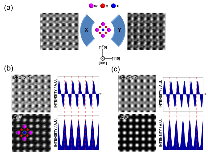
Fig. 1: (a) Schematic illustration showing the relationship between the crystallographic orientation of SrTiO3 and the two detector segments. (b) The DPC STEM image formed by subtracting the signal in detector segment Y from that in detector segment X and its image intensity profile [2]. |
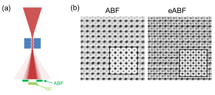
Fig. 2: (a)Schematic illustration of BF and ABF detector geometry. (b)ABF and eABF images of LaTiO3 observed from [001] direction [6]. |