IT-5-P-2448 A simple EDXperformance test for transmission electron microscopy
In the last 5 years solid angles increased dramatically (a factor 10 to about 1srad) and some systems are windowless further improving collection efficiency. In practice this means that for most elements a few percent (up to 10% for heavy elements) of the ionization events are now detected. Besides speeding-up conventional X-ray analysis (point analysis and 2D EDX elemental maps) large solid angle detectors have also enabled new EDX applications such as atomic resolution elemental mapping and 3D EDX tomography but this last application only on condition that X-ray collection is possible over a large sample tilt range (like for FEI’s Super-X™ detector).
Although the geometrical definition of a solid-angle is straightforward it is tedious to experimentally verify specified numbers and not all solid-angles yield the same detection efficiency. Some areas of the available real estate around the sample are better than others for X-ray detection and this leads to the concept of “quality of solid-angle” (see fig. 1). Here we propose to determine the quality of solid angle by measuring the output X-ray count-rate per nA of primary electron beam current on a very well-defined sample. This calibration sample needs to have an undisputable and stable composition over time, as well as a fixed and known thickness and must be easily and reliably produced in large quantities to allow for comparisons between systems.
In this study we propose to use 200nm thick Si3N4 windows made in 200μm thick silicon wafers and cut into 3mm discs to fit in regular low-background TEM holders (see fig. 2). Wafer processing technology ensures very good thickness uniformity and thickness reproducibility. Furthermore Si3N4 is stoichiometric and stable certainly when the membrane is 200nm thick and the electron beam is defocussed. Last but not least each wafer yields over 300 TEM samples which keeps the price down and guarantees easy access and supply. Actual measurements will be discussed.
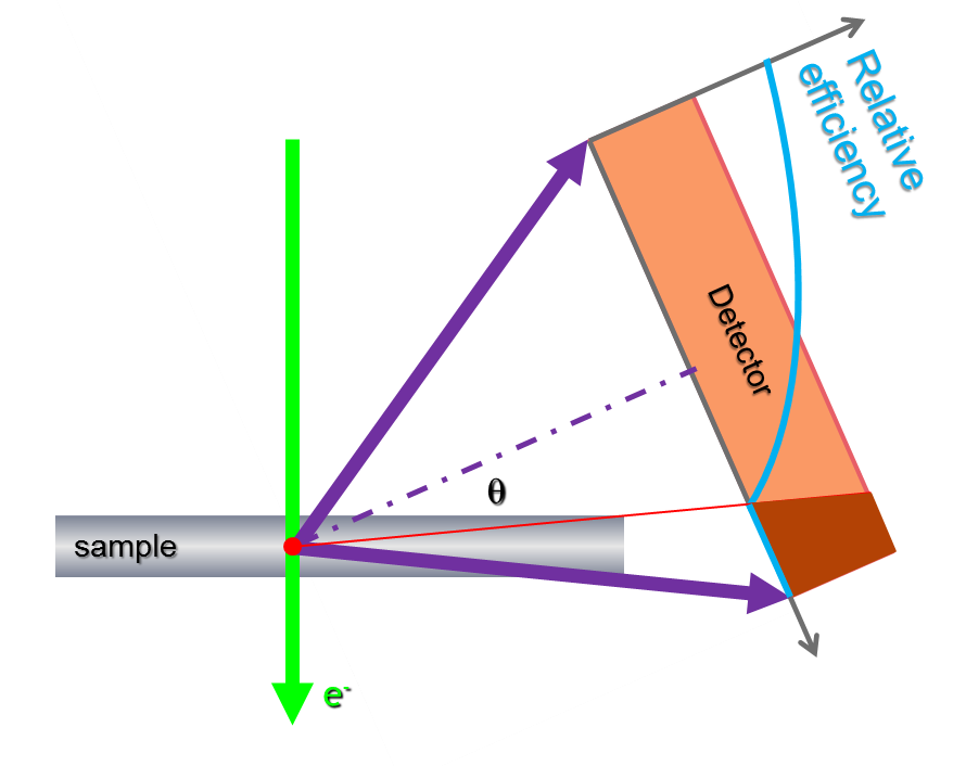
Fig. 1: A single large solid angle EDX: The average take-off angle is NOT θ as the lower part of the detector (dark area) doesn’t contribute at all to the signal. Below the red line no X-rays are counted and above the signal will gradually increase as the take-off angle increases (blue curve). |
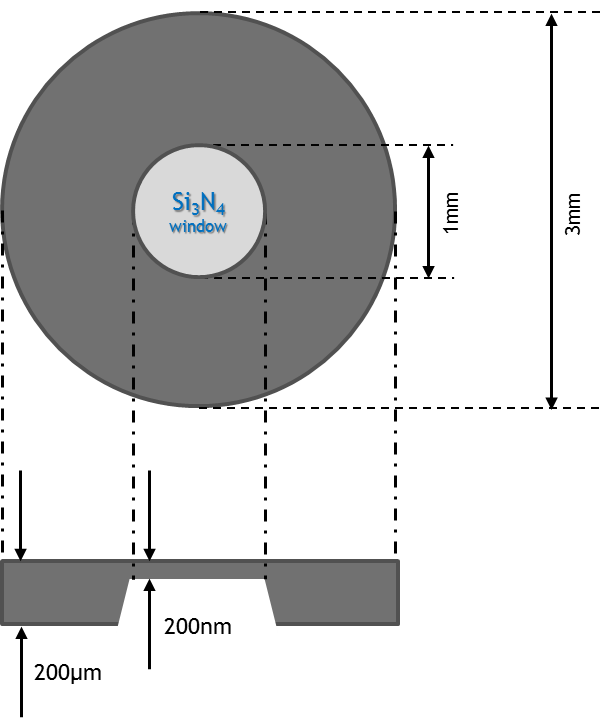
Fig. 2: The proposed sample: a Si3N4 window in a 3mm disc of 200μm thick silicon wafer, completely flat on the top to avoid shadowing. |