IT-11-P-2409 Low-keV electron microscope based on a single-atom electron source
Imaging of biological and organic molecules is a challenge in current electron microscopes due to insufficient contrast. Low-energy electrons emit from a single-atom tip1 (SAT) provide better contrast in light element materials and low radiation damage, and wave phases scattered from an object can be used to reconstruct images of the object due to its full spatial coherence2. Therefore, development of low-energy electron microscopes based on a reliable single atom emitter is highly desirable in study of light element materials.
We have built a low-energy electron point projection microscope (PPM) to evaluate emission characteristics of single atom emitter, as shown in Fig. 1. The beam divergence angle, measured at the half maximum intensity [Fig. 2(a)], becomes larger and the beam size at extractor becomes smaller with decreasing emitter-extractor separation [Fig. 2(b)]. This measurement may provide useful information for constructing an electron gun based on a single-atom source.
The beam energy used in PPM is always less than 500 eV and is not suitable for imaging molecules of 1 nm or thicker because the inelastic mean free path is less than 1 nm. Here we propose a low-keV (500 eV~ 5 keV) electron microscope based on a single-atom electron gun and a focusing lens, as shown in Fig. 3(a). In this electron energy range, samples with thickness of 3 nm or thinner can be imaged. It allows different imaging modes, including SEM imaging, coherent electron diffractive imaging, and holographic imaging.
A new challenge for the design is alignment. A narrow beam emitted from a single-atom source facilitates focusing, but also makes the alignment of the electron beam become critical, because misalignment by merely 1˚ causes a significant decrease in the beam intensity. Design for fine alignment of the source is essential for the successful extraction of the electron beam. Therefore, a piezo-stage with precision linear and angular adjustments is used to fine position the emitter. The custom-made stage enables building a compact and rigid system and provides the freedom to align and optimize the performance the entire system, as shown in Fig 3(b). Fig 3(c) presents a diffraction pattern of graphene with an imaging area around ~20 μm. We are improving the lens system to get better focusing of the system. This new instrument may allow determination of the atomic structures of individual thin nano-objects, such as graphene, carbon nanotubes, DNA molecules, or protein molecules.
Ref:
1. Nano Lett. 4 (2004), 2379.
2. Nanotechnology 20 (2009), 115401.
This work was sponsored by the Academia Sinica. We pay our great thanks to their financial support
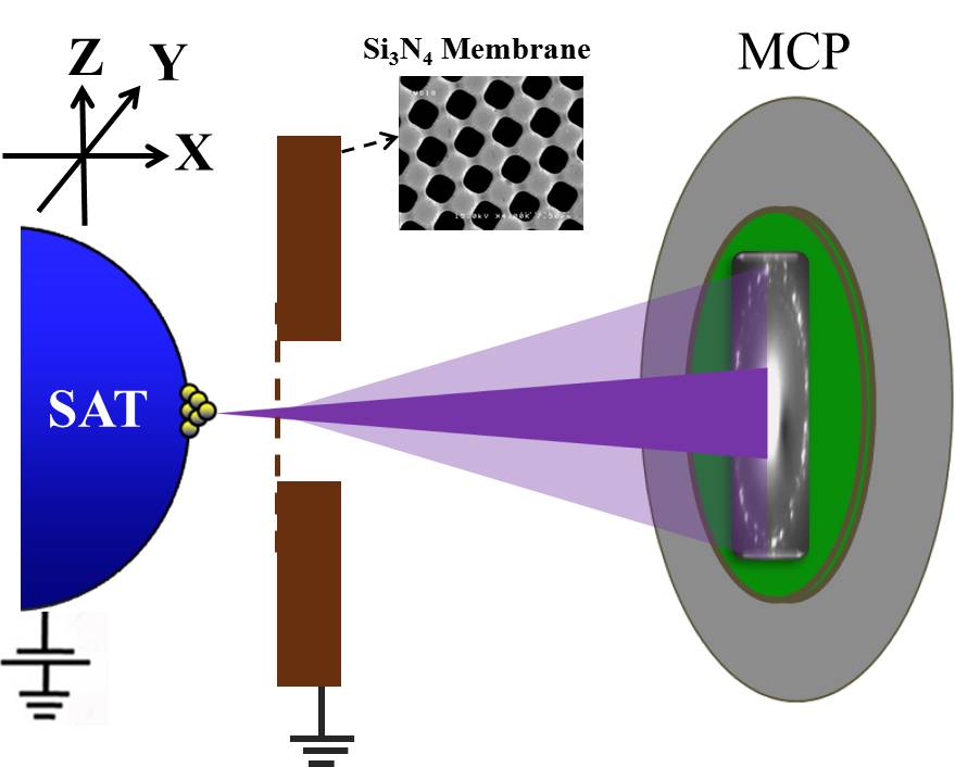
Fig. 1: Schematic diagram of a point projection microscope based on a single-atom emitter. |
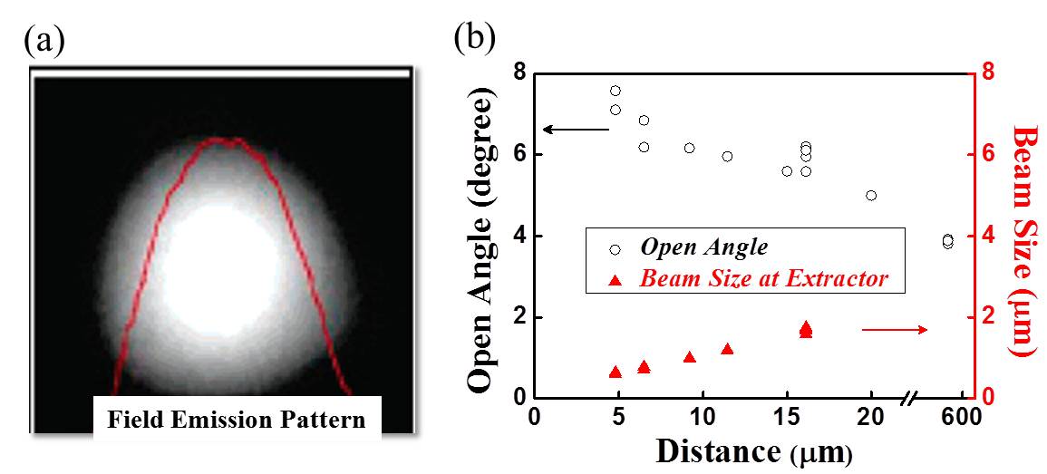
Fig. 2: (a) Intensity profile of an extracted beam from a single-atom electron source; (b) Opening angle & beam size v. s. the emitter-extractor separation. |
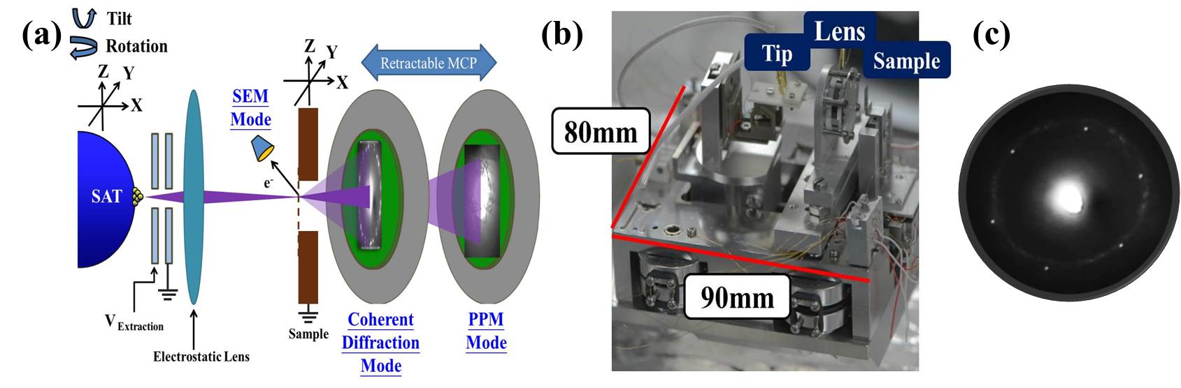
Fig. 3: (a) Schematic diagram of the low-keV microscope. (b) Photograph of the microscope. (c) Diffraction pattern of graphene. |
|