IT-5-P-2395 Toward X-ray Quantitative Microanalysis Maps with an Annular Silicon Drift Detector
The scanning electron microscope (SEM) was primary developed for imaging applications. With the introduction of the Si(Li) energy dispersive spectrometer (EDS), simultaneous imaging and x-ray microanalysis became possible. However, long working distance and high current were needed because the position and small solid angle of the EDS detector. SEM was initially and is still optimized for imaging applications, where the high spatial resolution is generally obtained at short working distance. This problem is still relevant today and unfortunately x-ray microanalysis is never performed in the best imaging conditions, i.e., not with the smallest probe size. The annular silicon drift detector (SDD) system is inserted below the objective lens and has four segments which give a higher solid angle (up to 1.2 sr). Also, a lower working distance and probe current can be used. An improved spatial resolution becomes possible during x-ray microanalysis. However, the effect of the detector geometry and position on the quantification microanalysis is unknown.
Because of the position of the detector, Mylar windows are used to prevent the backscattered electrons (BSEs) to damage the SDD segments. Three window thicknesses are available for this detector and their effect on the x-ray spectra is shown in Figure 1. The shape of the background was strongly affected by the window absorption at low x-ray energy. For accurate quantitative analysis, the calculation of peak net intensity depends on the background subtraction method used. Different approaches are currently studied with this annular SDD. Another artefact created by the window is the generation of C and O peaks and bremsstrahlung x-rays in the window by the BSEs. Figure 2 shows the variation of the output count rate for the spectrum and the Cu Lα peak with the working distance for the three window thicknesses. An optimum working distance was observed for the Cu Lα peak as predicted by the calculation of the solid angle of this detector. However, no decrease of the output count rate was observed. The x-ray emission in the window negates the effect of the solid angle. This effect is more pronounce at high accelerating voltage. An example of x-ray elemental maps of a mineral ore sample acquired with annular silicon drift detector (SDD) at low accelerating voltage is shown in Figure 3.
The effect of this detector geometry and position on the correction model is currently studied to obtain quantitative maps from the elemental maps. With adapted correction model, the annular SDD with its larger solid angle will clearly revolution the quantification microanalysis by moving from point analysis to quantitative micrograph with simultaneous electron imaging.
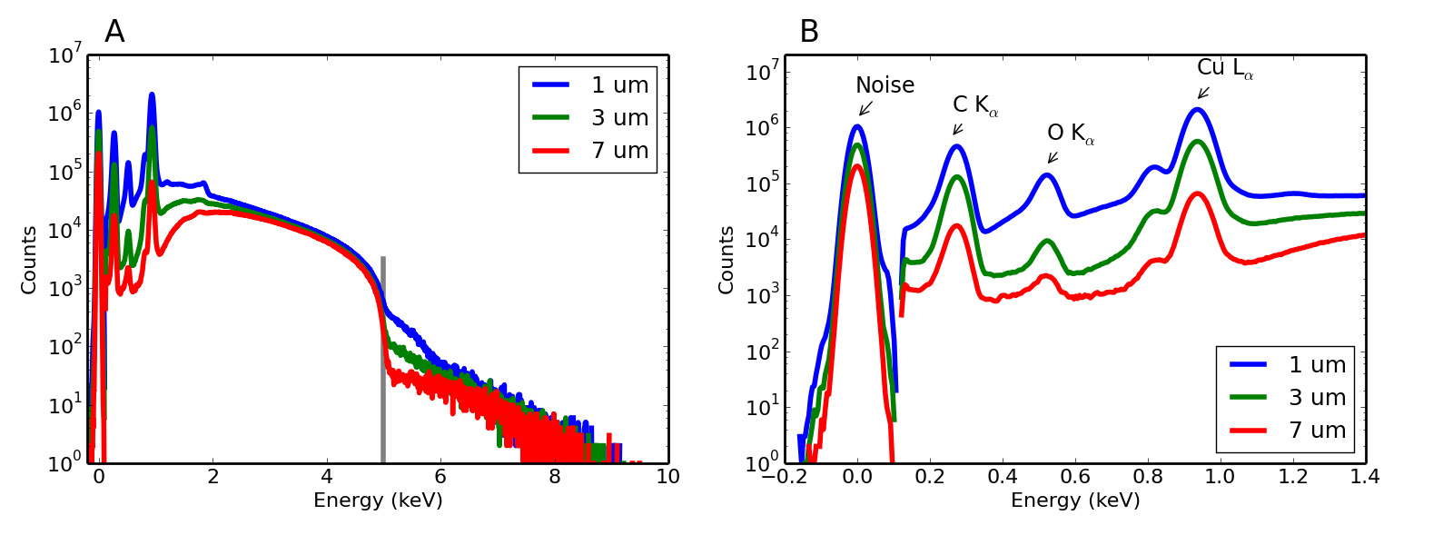
Fig. 1: Copper sample spectra with three different window thicknesses for annular silicon drift detector (SDD). The gray line shows the expected Duane-Hunt limit at 5 keV. The C Lα peak intensity decrease by 3.2 times with the 3 µm-thick window and 30 times with the 7 µm-thick window. |
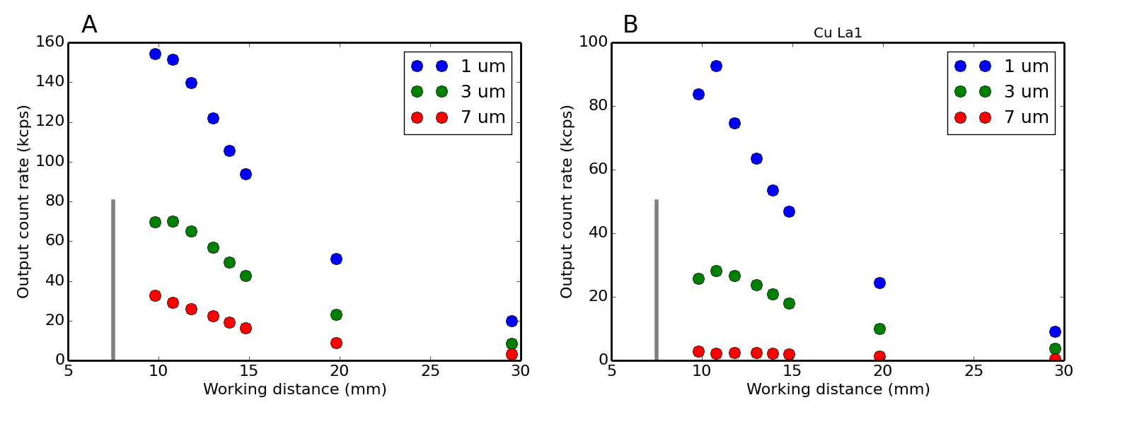
Fig. 2: Variation of the experimental output count rate with working distance for three different window thicknesses for annular silicon drift detector (SDD). The gray line shows the detector bottom position at 7.5 mm. |
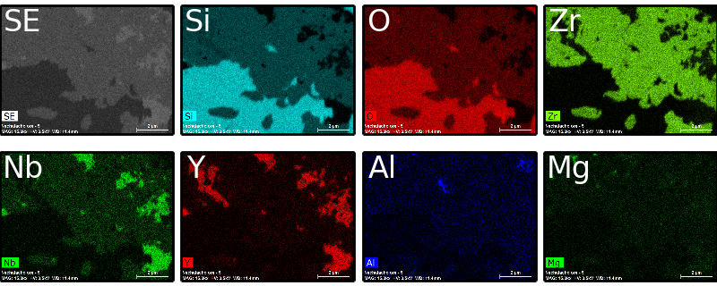
Fig. 3: X-ray elemental maps of a mineral sample acquired with annular silicon drift detector (SDD) at low accelerating voltage of 4 kV and working distance of 11 mm. The image size was 11 x 9 µm2 (1280 x 960 pixels) with an acquisition time of 1162 s (input count rate of 117.6 kcps). |
|