IT-5-P-2324 Band gap measurements of ultra thin buried films using conical darkfield EFTEM and low voltage EFTEM
New electronic devices require new techniques for characterization. We investigate a c-Si/a-SiOx/a-SiON/a-SiOx/pc-Si (SONOS) stack as used in flash memory devices by using valence electron energy loss spectrometry (VEELS) and energy filtered transmission electron microscopy (EFTEM).
In the present work we discuss the given physical limitations, which include relativistic energy losses – like Čerenkov losses – and the wide range Coulomb interaction. Whereas the first effect can alter the VEELS spectrum and can be easily avoided by reducing the beam energy, the latter affects the spatial resolution of the inelastically scattered electrons.
Although the range of the Coulomb interaction is smaller for slower electrons, the spatial resolution of the low voltage (LV-) EFTEM method will still be limited by this effect. In the case of conical dark field (conDF-) EFTEM we are going to locate the collection aperture in the reciprocal plane such, that we do not collect the small angle dispersed Čerenkov losses and such that we probe the indirect gap of Silicon. Still this method is critical, because its results do not give the optical properties. This is because the measurement is performed at q ≠ 0.
The EFTEM data cubes are recorded with a TECNAI G20. For the respective experiments we chose 40 keV for the LV-EFTEM experiment and 200 keV for the conDF-EFTEM experiment. In conDF the incoming electron beam is deflected by the Bragg angle of Si(111) and conically rotated during the EFTEM acquisitions. Therefore only dark field signal is used for the data cube.
Although the 40 keV experiment does not show Čerenkov losses inside the oxide-oxynitride-oxide (ONO) stack, it still shows some intensity in the direct gap of Silicon. Anyhow, the inelastic delocalization hinders an extraction of an SiO2 EELS signal. The major components of the spectrum extracted from the SiO2 layer positions are due to Si and SiON. The measured band gaps are 3.8 eV in SiON, 3.8 eV in SiO2, and 1.8 eV in Si (although the direct gap at 3.4 eV should be probed). They are all wrong due to delocalization and Čerenkov loss excitation.
In the case of the 200 keV conDF-EFTEM experiment, the spectra can be extracted quite well, although the SiO2 spectrum still suffers slightly from inelastic delocalization. The measured band gaps are 4.9 eV in SiON, 6.3 eV in SiO2, and 1.3 eV in Si (which is the indirect gap being probed under conDF conditions). The value for SiO2 still suffers from delocalization.
We demonstrate that the determination of optical properties of low is a problem with EELS as soon as the layer thickness is smaller than the inelastic delocalization. Probing the band gap can be done under the restrictions of a dark field experiment measuring q ≠ 0.
The authors acknowledge the USTEM facilities for providing the low-kV TEM.

Fig. 1: Figure 1: (a) Defocused bright field image of the area of interest. The ONO stack of the SONOS-transistor is located between the substrate and the pc-Si gate electrode. (b) elemental map of Silicon (green), Oxygen (blue) and Nitrogen (red). (c) HRTEM image of the ONO stack. |
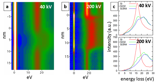
Fig. 2: Figure 2: (a) 40 keV spectrum image across the ONO stack extracted from the LV-EFTEM data cube. (b) 200 keV spectrum image across the ONO stack extracted from the conDF-EFTEM data cube. (c) Spectra of Si, SiO2 and SiON extracted from the corresponding data sets. |