IT-4-P-2277 Physical background of multiple detection possibilities of the Hitachi SU8030 SEM
The spatial resolution of state-of-the-art high resolution scanning electron microscopes has nearly reached the physical limit of around 1 nm. On the one hand, this has been achieved by optimised electron sources and improved low kV electron optics. On the other hand, advanced and multifunctional detectors have been developed to detect separately energy- and angular-selective secondary electron (SE) as well as backscattered electron (BSE) signals with reduced interaction volumes. While early SEMs used one SE- and one BSE-signal only, a fully equipped modern HRSEM offers the possibility to record up to 20 different signals. Therefore, the skilled operator will find the most suitable detection method to optimise the contrast of the nm-structures under investigations, no matter if they show up due to potential-, edge-, binding energy-, working function-, Z-contrast or anything else.
The aim of this work is the quantitative analysis of nm-structured samples, i.e. all possible signals should be linked to the analysed sample properties and to the physical background of the detection process. Due to the large variety of parameters, this was performed by analysing known samples with the different detection methods of a modern Hitachi SU8030 SEM.
As an example, fig.1 shows a Si-chip with conductive Si-tracks and isolating SiO2-areas around. On top, there is a PMMA polymer layer with cracks. On sample areas, consisting of polymer coating on Si substrate, both detectors, the lower one (mounted at the specimen chamber) and the upper detector (in-lens), show the same image contrast, which in this case is a pure element contrast. On SiO2 substrate, however, using the lower detector to display the cracked polymer leads to the same image contrast as before, whereas the upper detector additionally shows the potential contrast since it records a pure SE1-signal.
Fig.2 shows a Si wafer with square Au pads with 130 nm height. The images are taken with the top detector, which is located well above the upper detector. In non-deceleration mode, a high angle BSE signal is detected with orientation- and Z-contrast (fig. 2b). In deceleration mode, a negative voltage is supplied to the sample decelerating primary electrons as well as accelerating escaping secondary electrons, which subsequently will then be detected with the top detector. In the latter case, the pure SE-signal shows a fine topographic contrast (edges of Au-pads and grain boundaries) and it is sensitive to the surface potential (bright lines in the grooves, fig. 2a).
Further sample properties might be analysed, if primary electron energy, deceleration voltage, detected energy and WD are varied in addition. Consequently, a state-of-the-art SEM provides many complementary imaging modes utilizing its high flexibility.
We kindly acknowledge financial support from the Deutsche Forschungsgemeinschaft (DFG).
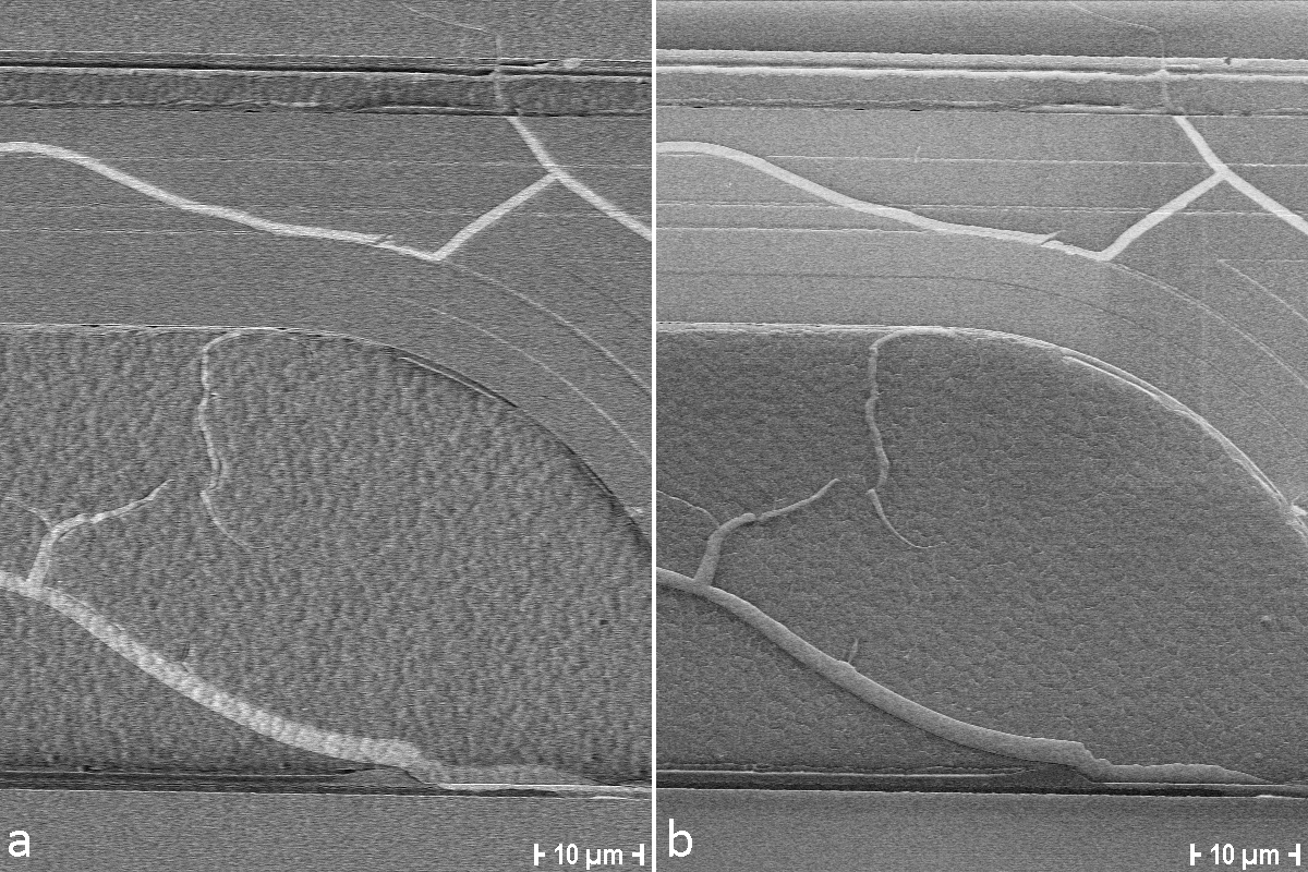
Fig. 1: Si-chip analysed with Hitachi SU8030 SEM. a: Lower detector (SE[L]); accelerating voltage 900 V; working distance 10 mm b: Upper detector (SE[U]); accelerating voltage 900 V; working distance 10 mm |
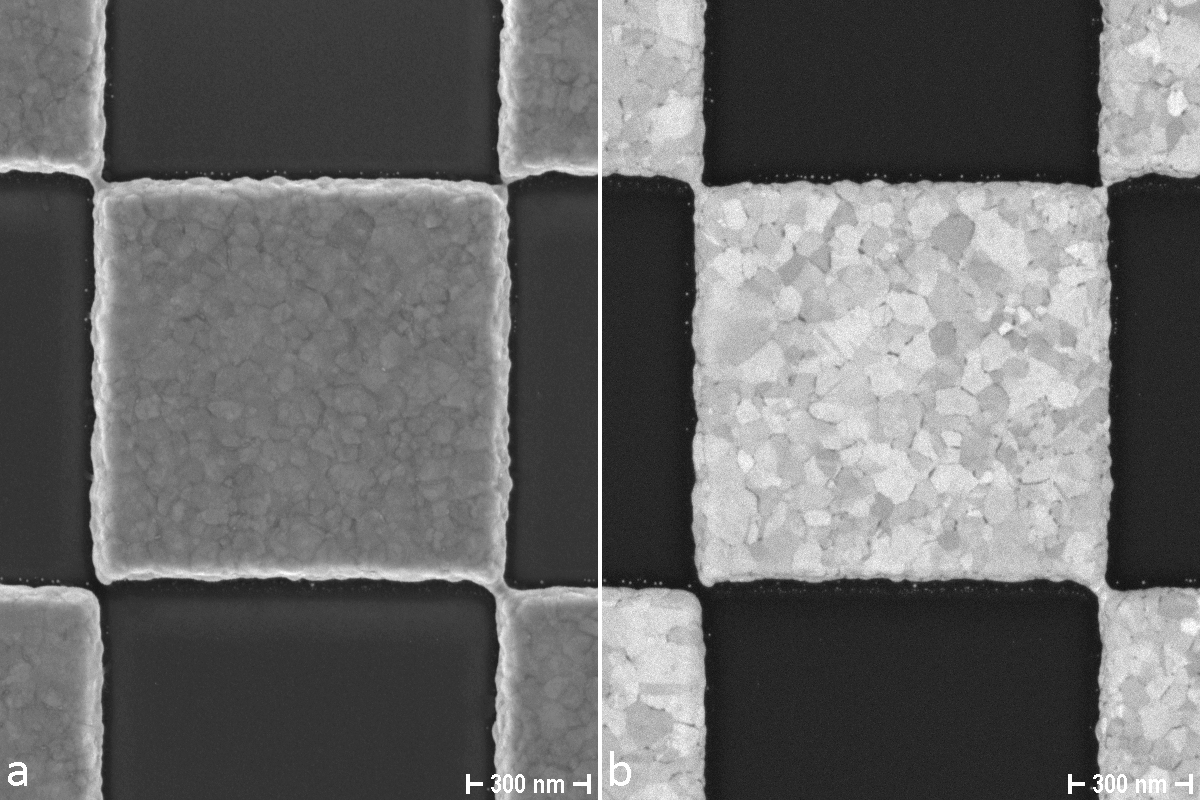
Fig. 2: Au-pads on silicon analysed with Hitachi SU8030 SEM. a: Top detector (SE[T]); landing energy 2 keV (accelerating voltage 3 kV; deceleration voltage 1 kV); working distance 1.9 mm b: Top detector (HA100[T]); landing energy 2 keV (no deceleration); working distance 1.9 mm |