IT-2-P-2265 Adding the Third Dimension to Atomic Resolution Spectrum Imaging
Aberration correction made possible two-dimensional atomic resolution spectrum imaging in the scanning transmission electron microscope (STEM). It also led to a significantly reduced depth of field which has been utilised to perform optical sectioning with atomic number contrast annular dark field (ADF) imaging and determine the positions of individual dopant atoms in three dimensions. Here we combine these corollaries of aberration correction to demonstrate three dimensional elemental mapping with atomic resolution electron energy loss spectroscopy (EELS). Atomic lateral resolution is critical as the optical transfer function of the STEM has a large missing cone, leading to excessive depth elongation for laterally extended objects [1]. The longitudinal resolution varies with the lateral spatial frequency. In regions relevant to lateral resolutions achievable today, the missing cone causes the longitudinal resolution to vary as approximately d/α where d is the characteristic spacing of the object and α is the convergence angle. If the highest spatial frequency resolved is for example the width of a 3 nm nanoparticle, the depth resolution will be around 136 nm with a 22 mrad convergence angle. If instead we were able to resolve atomic columns with a spacing of 0.3 nm and use a 30 mrad convergence angle the depth resolution improves to 10 nm. This relationship between lateral spatial frequency transfer and depth resolution applies both to ADF and EELS imaging. However, although theoretical simulations suggested it was possible to perform optical sectioning with EELS, it had not previously been demonstrated experimentally.
Using a Nion UltraSTEM 100 operated at 100 kV with a 30 mrad convergence angle we acquired successive spectrum images from the same area of a sample, but with the probe focused to different depths. The EELS optical sectioning revealed the presence of a network of yttria-stabilized zirconia (YSZ) islands buried beneath strontium titanate (STO). These regions appear perovskite like from 2D imaging focused at the entrance surface, emphasising the importance of considering the possibility of three dimensional inhomogeneity. The results also highlight the unambiguous nature of EELS elemental mapping, revealing 3D compositional changes that cannot be determined through ADF optical sectioning with complete certainty.
[1] G. Behan et al, Phil. Trans. R. Soc. A 367 (2009), p. 3825.
SuperSTEM is the EPSRC UK National Facility for Aberration-Corrected STEM. Research at ORNL was sponsored by the U.S. DOE, Office of Science, Materials Sciences and Engineering Division (MV). The research leading to these results has received funding from the European Union Seventh Framework Programme under Grant Agreement 312483 - ESTEEM2 (Integrated Infrastructure Initiative–I3).
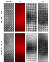
Fig. 1: Optical sectioning with atomic resolution spectrum imaging. The Sr (M-edge), Ti (L-edge) and Zr (M-edge) maps have been denoised with principle component analysis, and are shown alongside the simultaneously acquired high angle annular dark field (HAADF) images. |