IT-5-P-2235 The Use ofVery Large Area Detectors for fast Light Element Mapping and Data Acquisition in STEM
In recent years silicon drift detectors have become the logical choice for characteristic EDS X-ray analysis in both SEM and TEM. Large sensor sizes offer increased solid angle, allow data to be acquired faster in low signal regimes and with only Peltier cooling required, the need for liquid nitrogen is removed. High count rate situations are also handled more easily due to lower noise and excellent energy resolution.
Now ultra-large non circular SDD detectors have been designed for (S)TEMs. With their non-traditional geometries, they minimize the detector to sample distance and give very high solid angles. These large EDS detectors are able to detect and map elements down to the atomic level whilst minimizing analysis times and thus limiting the effects of beam drift, beam damage and sample contamination.
By taking further advantage of the clean, high vacuum regimes present in modern field emission (S)TEMs and the fact that these new detectors may be operated at relatively high temperatures, windowless SDD detectors can also now be easily and safely incorporated as part of the analytical system.
By dispensing with the window and support grid, not only is true solid angle increased, but the increased collection efficiency dramatically improves signal to noise ratios for lower energy X-rays such as NKα and OKα. Figure1 shows this huge improvement in light element performance for the new Oxford Instruments X-MaxN 100TLE detector compared to an 80mm2 SDD detector.
This improved performance is especially useful for TEM instruments without EELS capabilities, where light element analysis can be problematic. Sensitivity can be further increased by mounting more than one detector on suitable instruments – this can maximize solid angle up to 2.0sr. Not only is collection efficiency for un-tilted samples increased, but it also gives the ability to tilt the sample in a negative direction which can be useful when collecting simultaneous diffraction data.
Figure 2 shows an example of elemental distribution in an LED nanowire taken with a single X-Max 100 TLE in 10 minutes and structures as small as 2nm can be identified. The Al and Ga distribution is well defined and N concentrations are evenly distributed throughout the wire. In addition a thin out coating of oxide only a few nanometers thick is clearly seen in the mapping data. High resolution maps such as these can be collected in just 5 -10 minutes using a single detector.
Conclusions:
Large solid angle windowless detectors extend the capabilities of EDS analysis to application areas which were formerly regarded as being limited to EELS only. Higher collection efficiencies, especially at low energy now makes EDS a truly viable option for light element analysis on the nanoscale.
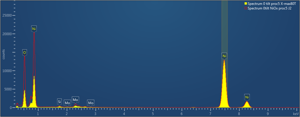
Fig. 1: Comparison of X-Max 80T (yellow - 80mm2 window) and Maxᶰ 100TLE (red - 100mm2 very large solid angle windowless) SDDs. Spectrum has been normalized on the Ni Kα peak to show the sensitivity enhancement of the windowless operation for low energy X-rays. |
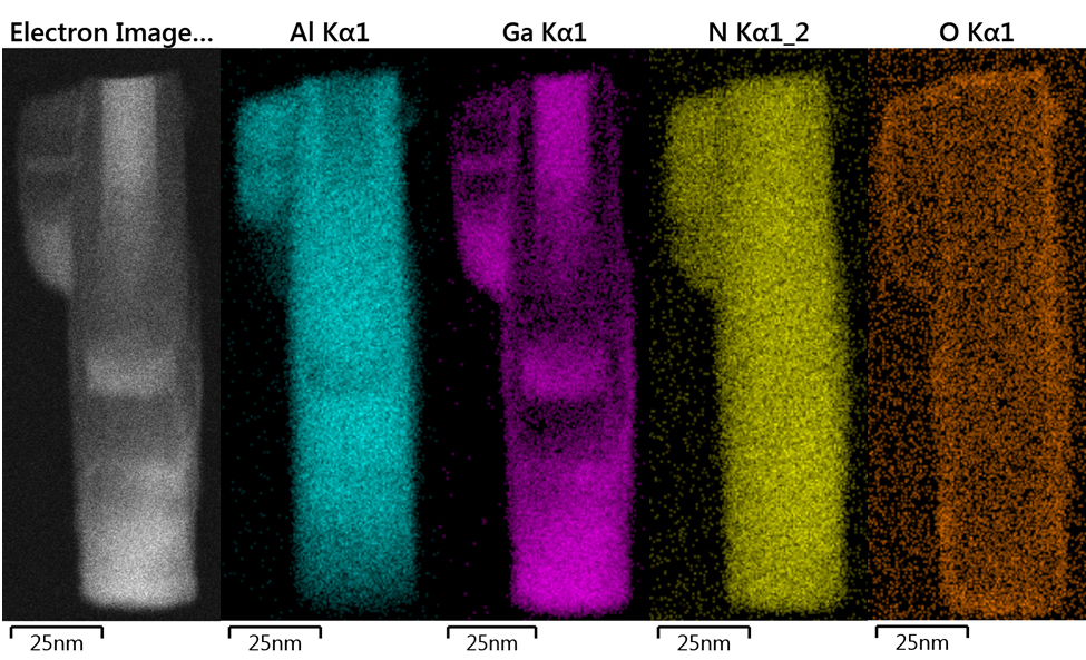
Fig. 2: Mapping of LED Al-Ga-N nanowires showing the elemental distribution throughout the wire. Each map has a resolution of 266x113 pixels. |