IT-11-P-2202 Toward a 3D strain mapping at nanometer scale with Dark-Field Electron Holography
Dark-Field Electron Holography (DFEH) is a technique developed to map strain at the nanometre scale with a large field of view. The principle is based on measuring the variation phase of diffracted beam due to small strain which is the so called geometric phase1. Due to the diffraction conditions used for obtaining dark-field holograms, it is not possible to combine classical electron tomography with DFEH as it was done with electron holography for 3D magnetic and electric field mapping. Until now and similarly to GPA, two diffracted beams were selected to map 2D strain field projected on the electron direction. Here, we propose to combine 3 or 4 non collinear diffracted beams to reach the 3D strain map of a multilayer sample constituted by the repeated stacking of SiGe/Si layers grown along the [001] direction.
In order to keep the same dynamical conditions, all the diffracted beams belong to the {220} family. Two of them (0-22) and (02-2) are included in the [100] zone axis and two others (20-2) and (-20-2) in the 90° tilted zone axis namely [010] as shown in the Fig.1. Since DFEH imposes very strict constraints relating to the sample such as flatness and uniformity of the thickness on both reference and strain areas, specific FIB techniques have been developed for 2D strain mapping with DFEH. Here, we created a needle sample with a squared cross section in order to obtain a symmetric configuration and exactly the same thickness in both zone axis (Fig.2). The value of the thickness was chosen such that the crystalline thickness corresponds to a half integer of the extinction distance2 ξ220 and that the field of view was large enough.
The strain maps corresponding respectively to [100] and [010] are presented in the Fig.3. Since sample edges yield relaxation effects which are even stronger in strain regions, the measured profiles does not exactly correspond to the expected bulk values. However, the similarity between the strain profiles from both zone axis proves of the symmetry of the boundary conditions. All the projections that are required to reconstruct the 3D strain map are now known and the information common of both zone axis serves to validate the method.
In this study we present a method yielding for the first time a 3D reconstruction of the strain at nanometer scale. These results are also compared with the new 2-beams theory considering dynamical effects and resulting simple projection rule for the measurement of the geometric phase within the thickness. To carefully develop this method we chose a well characterized strained sample, however, the scope of this new technique is of high importance for entirely controlling the electron mobility of new nano devices.
1.M.Hÿtch et. al Nature453(2008)
2.A.Lubk, E.Javon et. al Ultramic.136(2014)
The authors acknowledge financial support from the European Union under the Seventh Framework Program under a contract for an Integrated Infrastructure Initiative (ESTEEM2) and the French National Agency (ANR) in the frame of its program in Nanosciences and Nanotechnologies.
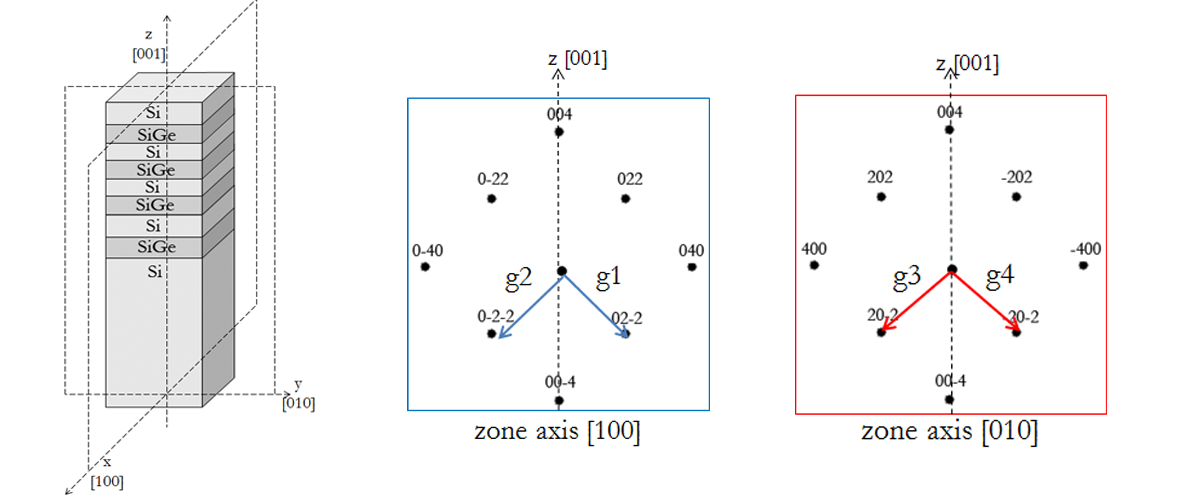
Fig. 1: Schematic illustration of the needle preparation: a squared cross section yielding the same thickness in both [100] and [010] zone axis. |
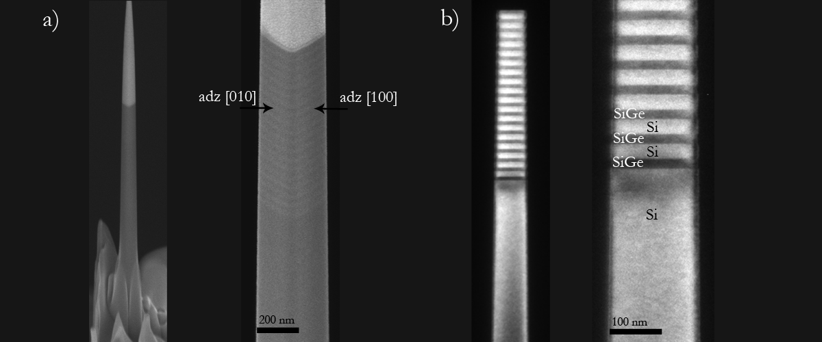
Fig. 2: (a) SEM image of a FIB of the squared needle. (b) Conventional dark field image of the multilayer SiGe. |
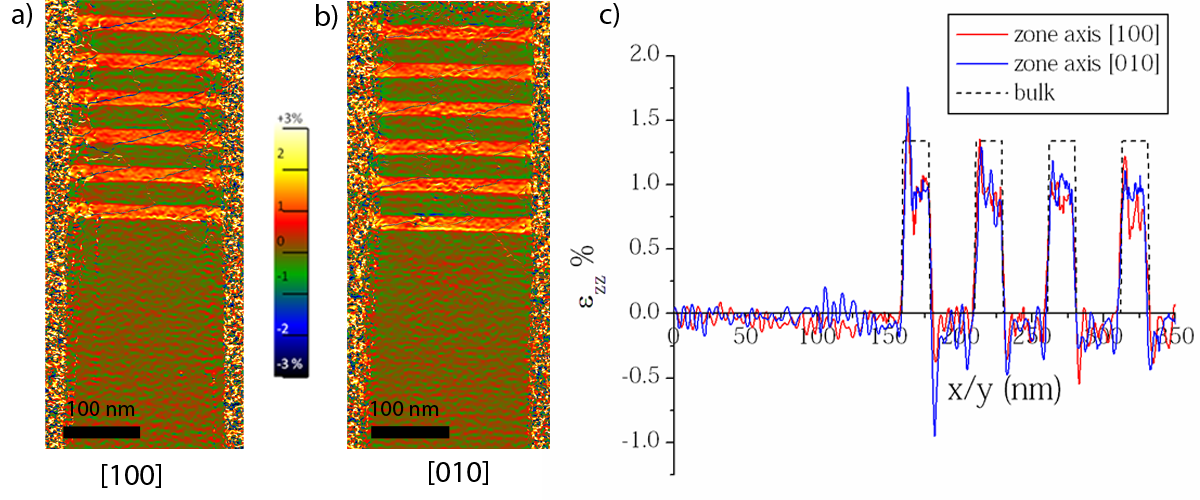
Fig. 3: Strain map εzz corresponding respectively to the (a) [100] and (b) [010] zone axis. (c) Comparison of both strain profiles from the [100] and [010] zone axis along the [001] direction with the bulk value. |
|