IT-5-P-2169 QW emission shift along single InGaN/GaN core-shell LEDs evaluated by monochromatic cathodoluminescence image series
Three dimensional light emitting diodes (LEDs) with a shell geometry of p-GaN and InGaN multi quantum well (MQW) around a columnar n-GaN core are supposed to have distinct advantages over conventional planar LEDs. The active area along the sidewalls of the GaN pillars can substantially be increased by high aspect ratios - leading to a lower current density inside the MQW at the same operating current per substrate area.
The investigated core-shell LED structures are grown by selective area metal organic vapor phase epitaxy on templates consisting of a patterned SiOx mask layer on an n-type GaN layer on 2” sapphire wafers. Due to the 3-dimensional shape, the optical properties of the QWs in each structure show significant gradients along the height and variations between different facets on a micrometer scale.
The automatized capturing of monochromatic CL image series is realized by combining a scan generator (controlling the electron probe position on the sample) and monochromator control (grating rotation angle). Hyperspectral imaging as well as spectra from selected areas are generated by post processing of such image series with respect to the spectral sensitivity of the optical system - including the collection optics, monochromator and detector. The spatial 2-dimensional (2D)-resolution of the presented method is higher than that of using a parallel detector for capturing CL spectra for distinct points of excitation. In parallel, the flexibility of the wavelength range gives a benefit for hyperspectral investigation in different regions of emission from the 3D InGaN/GaN LEDs.
The CL shows near band edge emission (NBE), signals from the QWs and defect related yellow luminescence (YL) which proves that the InGaN is present on all sidewall facets. The properties of neighbor structures are similar – although their diameters might be different. By contacting a single facet with a tungsten probe tip electroluminescence (EL) spectra are obtained at different injection currents.
Investigation of those structures by electron beam induced current (EBIC) proves the geometry of a p-shell around an n-core. Similar to the CL intensity the spatially resolved EBIC analysis indicates how the generation rate is affected by topography (edges) and that the top facets show different properties. A wavelength shift of the MQW emission of 60 nm is observed along the structure height for both excitations by the electron probe (CL) and by a local current injection (EL). This shift is assigned to a gradient of the indium incorporation caused by diffusion mechanisms during growth.
We thank Dr. Uwe Jahn for support regarding optical characterization. The financial support of the European commission (SMASH and GECCO) and the endorsement of the NTH and the JOMC are acknowledged.
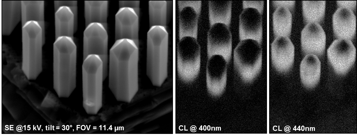
Fig. 1: SE image and monochromatic CL images of InGaN/GaN core-shell LED structures on the cleaved growth template using a spectral FWHM of about 7.5 nm at an FOV = 11.4 µm, EHT = 15 kV, tilt = 30°. |
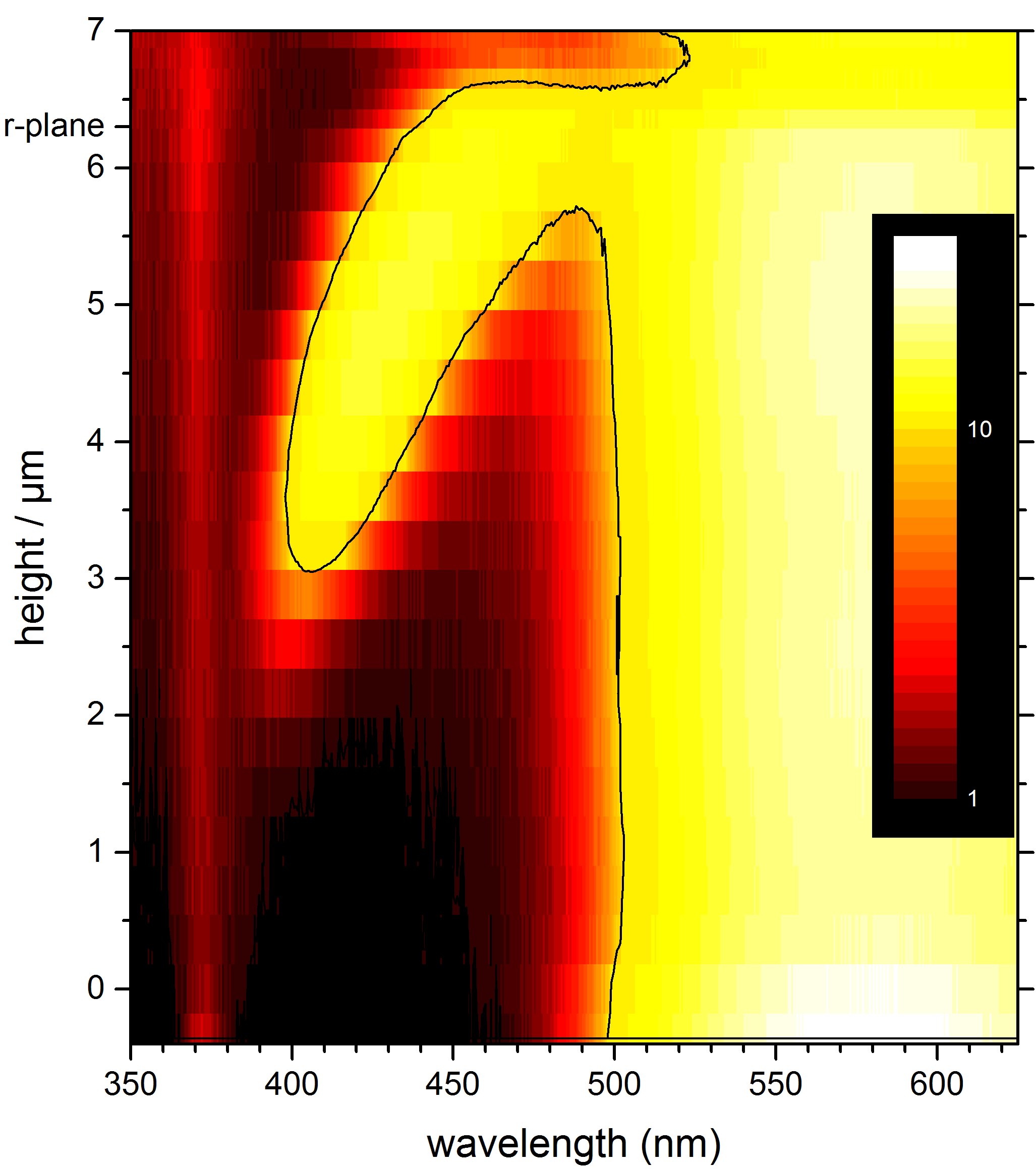
Fig. 2: Logarithmic contour plot of CL spectra obtained by exciting small areas at different structure height (17 positions on the sidewall and 6 positions on the top facets), captured with a spectral FWHM of about 7.5 nm using a CCD parallel detector. |
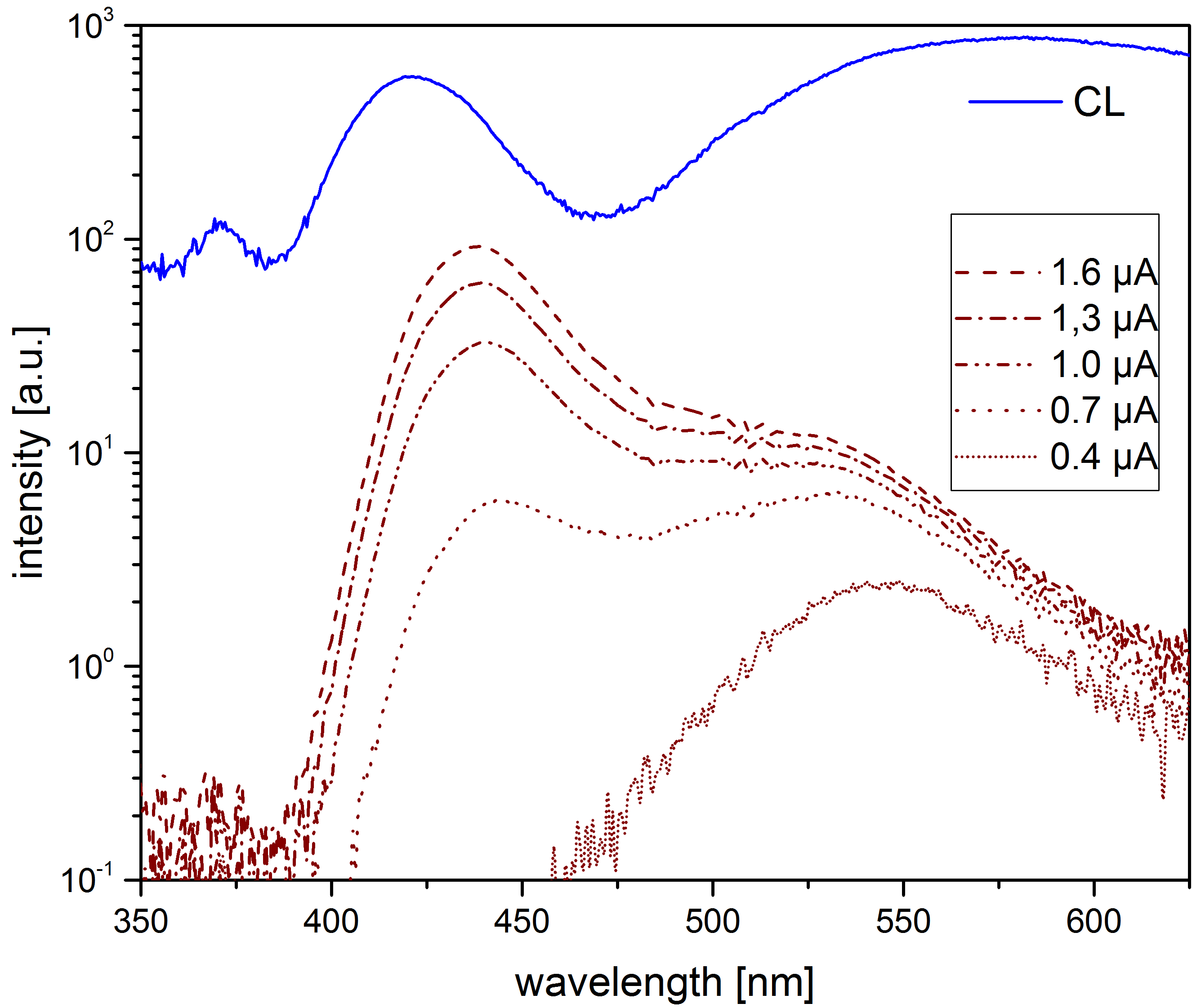
Fig. 3: CL and EL spectra captured with a spectral FWHM of about 7.5 nm using a CCD parallel detector. The single core-shell LED was excited at different heights on the sidewall by an electron probe of EHT = 15 keV and a current injection of I = 1.5 µA via a probe tip contact, respectively. |
|