IT-5-P-2130 Plasmon Mapping in Au@Ag Nanocube and their assemblies
Plasmons are collective excitations of conduction electrons in metallic particles. For nanostructures, the resonant surface plasmon modes are highly sensitive to the geometry of the structure and can therefore be tuned by controlling their morphology and/or size. Here, we applied monochromated STEM-EELS to map the surface plasmon resonances in Au@Ag nanocubes and their assemblies. [1]
These assemblies reveal interesting plasmonic properties with an increased flexibility as compared to their single particle counterparts.
For the isolated nanocubes, EEL spectra were recorded at different locations, revealing the presence of three distinct plasmon resonances at energy values of 2.2 eV, 3.2 eV and 3.5 eV. As presented in Figure 1, the extracted plasmon maps indicate that the two modes with the lowest energy have the highest probability to be excited at the corners of the particles, whereas the third mode is best excited at the side faces, in agreement with previous reports. [2]
Interestingly, when the nanocubes are dispersed on a C support, they tend to orient themselves side by side yielding regular assemblies. As a first example, 3 nanocubes may form an approximately triangular array as shown in Figure 2. It can be observed that the main plasmon modes are obtained at energy losses of 1.2 and 1.6 eV and are in qualitative agreement to the plasmon modes of a perfect nanotriangle with the same dimensions. [3] Plasmon modes that occur at higher energy losses originate from the deviation of the overall shape from a perfect triangle, resulting in multiple regions of high intensity that are mainly located at the corners of the individual cubes. A nanotriangle constructed by the random ordering of multiple nanocubes could possibly act as the first half of a bow-tie antenna. This antenna has great potential due to the field enhancement in the central region between the two triangles caused by plasmon coupling. [4] As illustrated in figure 3, even with the simplified geometry for a bow-tie antenna, the field enhancement due to the coupling can be clearly visualized in the centre of both the experimental and the simulated plasmon maps. The enhanced field occurs at an energy loss of 1.3 eV which can also be observed as an increased probability for the energy loss in the acquired EEL spectra.
[1] S. Gómez-Graña, J. Phys. Chem. Lett. 4 (2013) p.2209
[2] O. Nicoletti et al., Nature 502 (2013) p.80
[3] J. Nelayah et al., Nature Physics 3 (2007) p.348
[4] A. Koh et al., Nano Letter 11 (2011) p.1323
The authors acknowledge support from the European Research Council and the FWO.
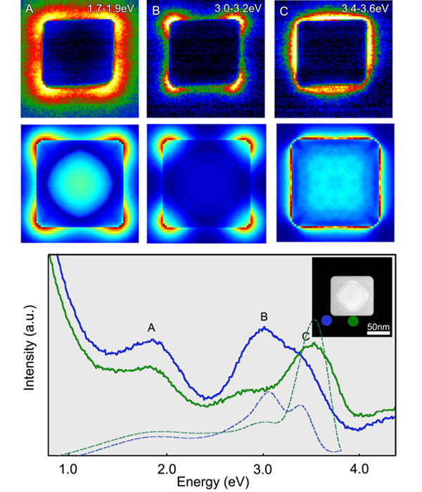
Fig. 1: Low loss EEL spectra of a Au@Ag nanocube showing three distinct major plasmon modes (a-c). The first two modes have the highest possibility to be excited at the corners of the cubes whereas the third one is best excited at the edges. |
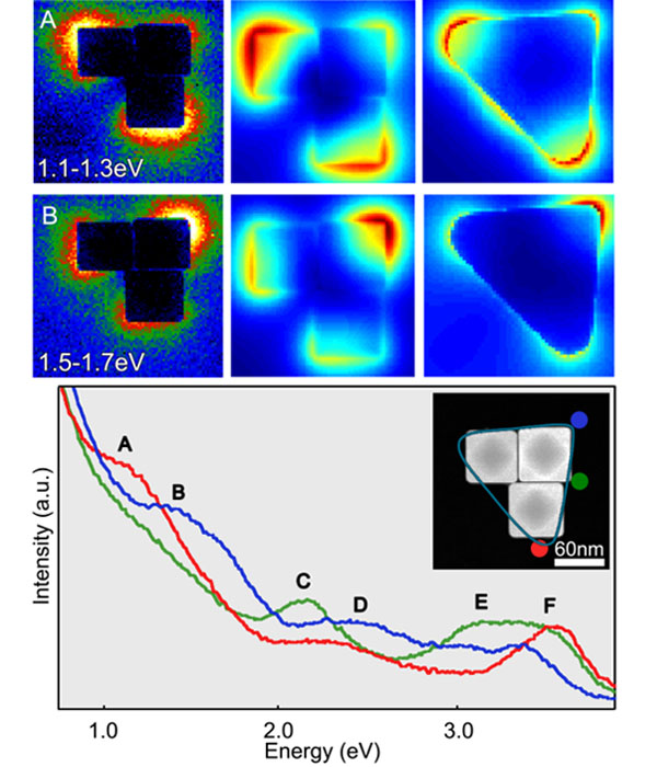
Fig. 2: Surface plasmon modes of a triangle comprising three Au@Ag core-shell nanocubes. (A and B) The EELS spectra were acquired at the positions indicated by the dots of the corresponding colors. When inspecting these spectra, several modes are observed, which are in agreement with BEM simulations of a perfect triangular shape. |
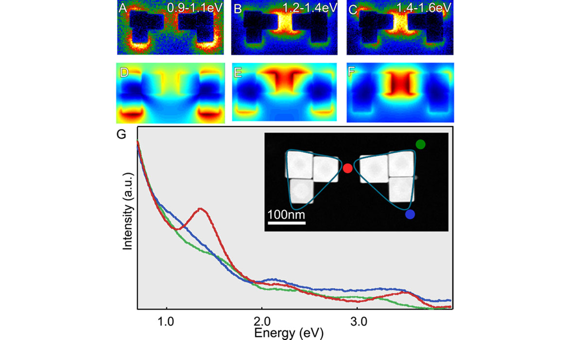
Fig. 3: Surface plasmon maps of a bow-tie antenna created by a specific order of self-assembled nanocubes. Both the acquired EELS spectra (A) and the experimental and simulated near field maps (B-G) show a large field enhancement in the region between both nanocube structures. |
|