IT-5-O-2097 Characterization of hybrid plasmonic waveguide by dispersion measurement
Dielectric waveguides combined with plasmonic waveguides, so called hybrid waveguides [1], have a great potential for providing subwavelength confinement and long propagation length, leading to highly integrated photonic circuits. The simplest example of the hybrid waveguide structures is a three-layered film consists of a high-permittivity semiconductor layer separated from a metal substrate with a thin low-permittivity insulator gap. We performed dispersion measurements on Si/SiO2/Al films using angle-resolved EELS (AREELS) combined with a TEM [2].
Figure 1(a) and (b) show AREELS patterns taken from the Si(157 nm)/SiO2(6 nm) film and the Si(157 nm)/SiO2(6 nm)/Al(35 nm) film, respectively. The dispersion curves of the first and second order Si waveguide modes are observed in Fig. 1(a), while the dispersion curves in Fig. 1(b) shift to the low energy side compared to those of the Si waveguide modes. These curves are the dispersion curves of the hybrid waveguide modes. According to the coupled-mode theory [3], to a first approximation, the hybrid waveguide mode can be described as a superposition of the Si waveguide mode and the surface plasmon-polariton (SPP) mode excited on the Al/SiO2 interface. The amplitude of the Si waveguide mode ASi is determined by the wave vector of the Si waveguide (kSi), the SPP (kSPP) and the hybrid waveguide (khyb) modes as follow [1],
|ASi|2 = (khyb-kSPP)/(2khyb-kSi-kSPP). (1)
Using the experimental dispersion plots (Fig. 2(a)) and the calculated dispersion relation of the SPP mode excited on the interface Al/SiO2, the square norm of ASi can be determined by equation (1). Figure 2(b) shows the resultant mode character depending on the energy of coupling. The hybrid waveguide mode with high energy has large component of the Si waveguide mode, so the electromagnetic energy of waveguide is mainly stored inside the Si layer, while it should be transferred from the Si layer to the Al/SiO2 interface with the decrease of energy because of the increase of the SPP component as shown in Fig. 2(b).
[1] R. F. Oulton et al. Nat. Photon. 2, 496 (2008).
[2] H. Saito et al. J. Appl. Phys. 113, 113509 (2013).
[3] A. W. Snyder and J. D. Love, Optical Waveguide Theory (Chapman and Hall, London, New York, 1983).
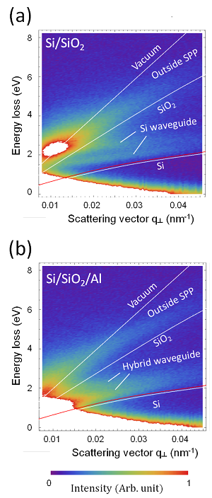
Fig. 1: Figure 1. AREELS patterns of (a) Si/SiO2 film and (b) Si/SiO2/Al film. The white curves and line are the calculated dispersion relations of light in Si bulk, SiO2 bulk and vacuum. The red curve is the dispersion relation of Čerenkov radiation in Si bulk. |
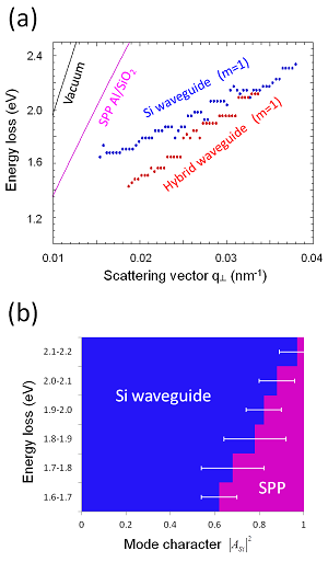
Fig. 2: Figure 2. (a) The dispersion plots of the first order modes of the Si waveguide obtained from Si/SiO2 film (blue) and the hybrid waveguide obtained from Si/SiO2/Al film (red). (b) The energy dependence of the square norm of ASi calculated using the equation (1). |