IT-1-O-2071 Sculpturing the electron wave function using nanoscale phase masks
Electron beams are extensively used in lithography, microscopy, material studies and electronic chip inspection. Today, beams are mainly shaped using magnetic or electric forces, enabling only simple shaping tasks such as focusing or scanning. Recently, binary amplitude gratings achieved complex shapes. These, however, generate multiple diffraction orders, hence the desired shape, appearing only in one order, retains little of the beam energy. Here we demonstrate a method in electron-optics for arbitrarily shaping electron beams into a single desired shape, by precise patterning of a thin-membrane. It is conceptually similar to shaping light beams using refractive or diffractive glass elements such as lenses or holograms - rather than applying electromagnetic forces, the beam is controlled by spatially modulating its wavefront. Our method allows for nearly-maximal energy transference to the designed shape, and may avoid physical damage and charging effects that are the scorn of commonly-used (e.g. Zernike and Hilbert) phase-plates. The experimental demonstrations presented here – two solutions to the free-space wave equation: on-axis Hermite-Gauss and Laguerre-Gauss (vortex) beams, and computer-generated holograms – are a first example of nearly-arbitrary manipulation of electron beams. Our results herald exciting prospects for microscopic material studies, research in electron-matter interaction, enables electron lithography with fixed sample and beam and high resolution electronic chip inspection by structured electron illumination.
The work was supported by the Israel Science Foundation, grant no. 1310/13 and the German-Israeli Project cooperation.
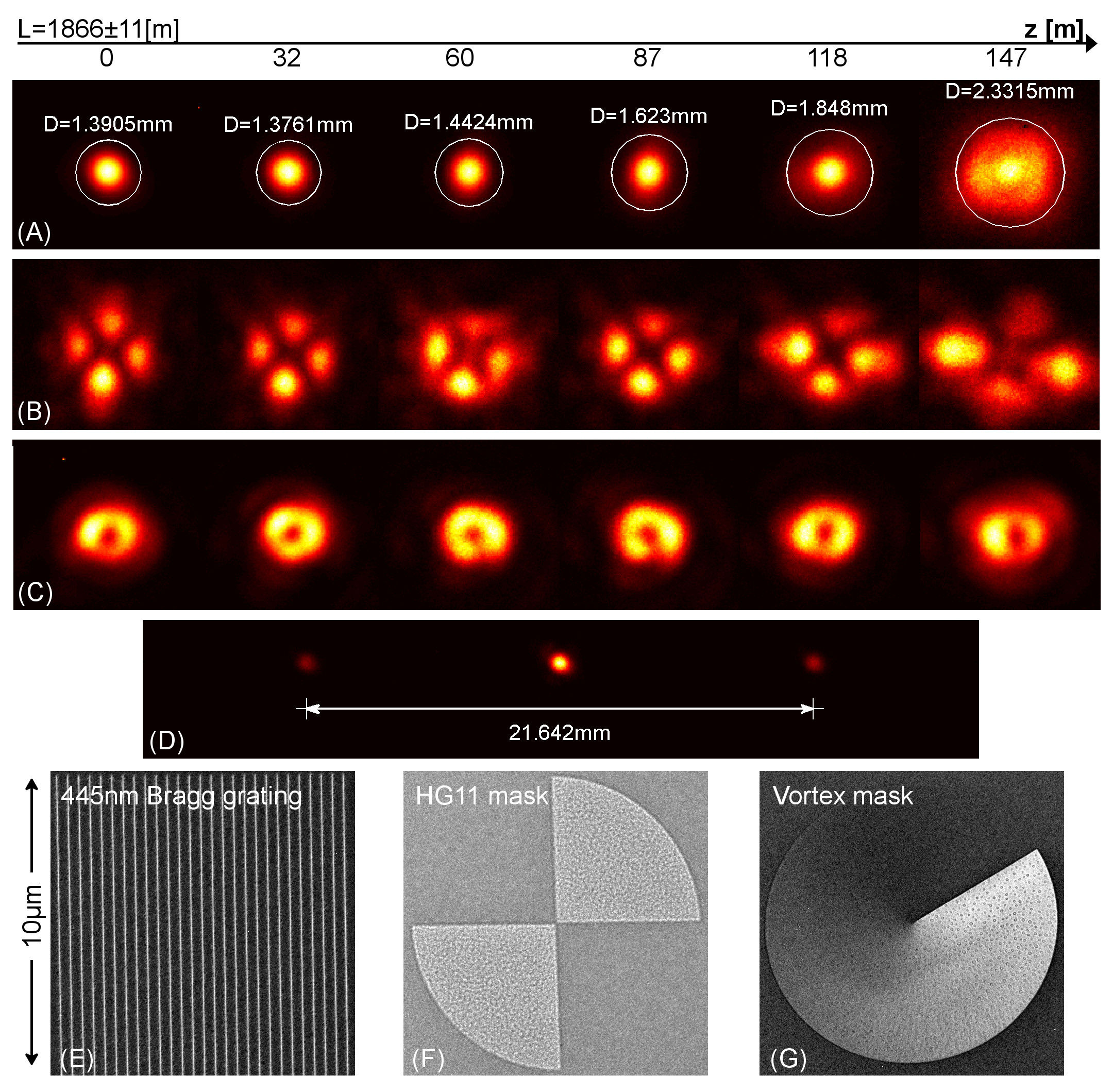
Fig. 1: On-axis generation free-space modes: images taken at different effective distances near the diffraction plane. (A) Unmodulated beam passing through the membrane, (B) Hermite-Gauss11-like, (C) Laguerre-Gauss01-like (vortex), (D) Bragg diffraction pattern used as metric, (E) Bragg grating, (F) HG11-generating mask, (G) vortex-generating mask. |
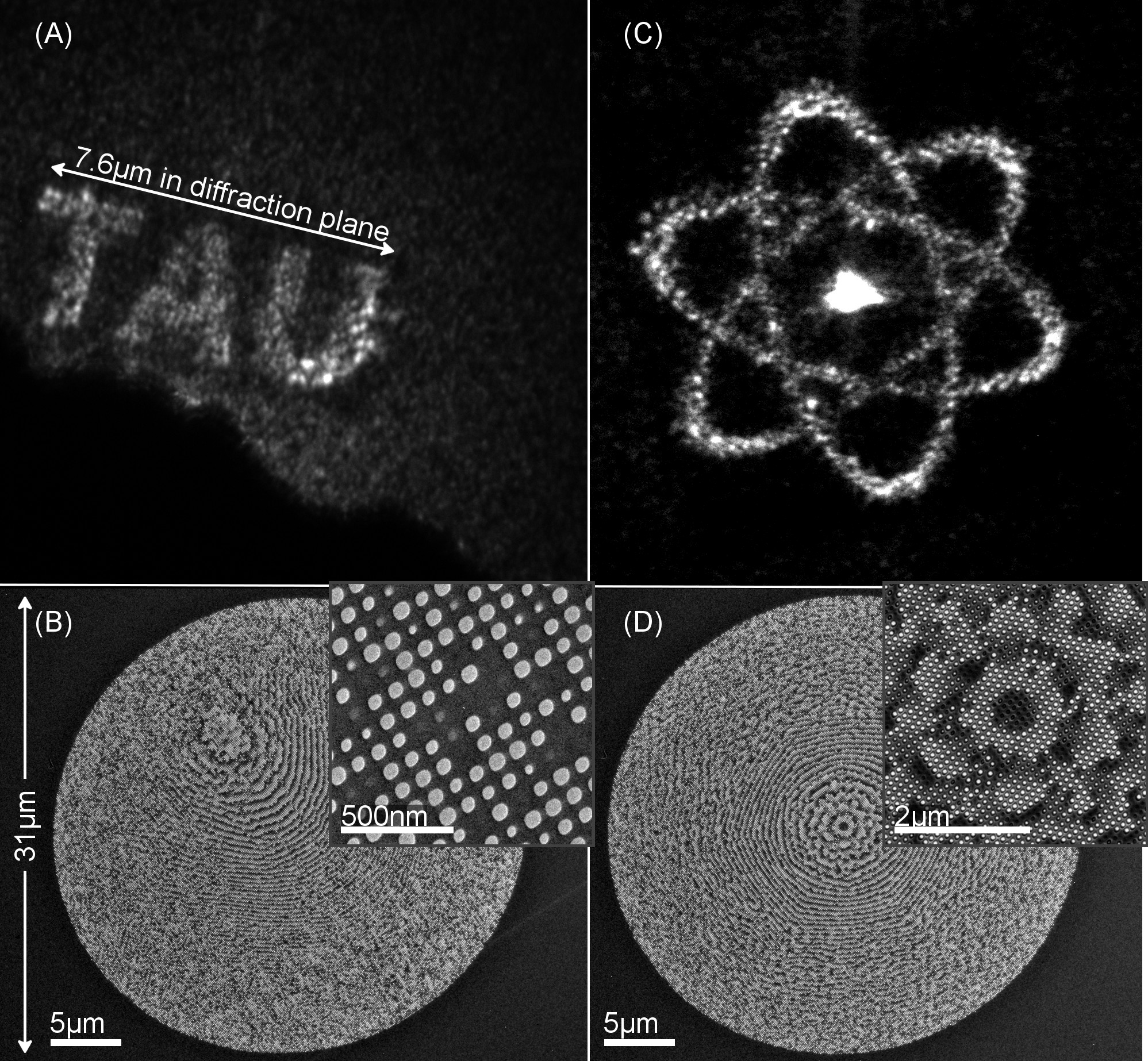
Fig. 2: On-axis holograms: (A) “TAU” hologram produced by the mask in (B); inset: magnification showing ~60nm holes composing the pixels. (C) Electrons orbiting a nucleus hologram produced by the mask in (D); inset: magnification showing the centre of the mask. Note: contrast and brightness levels in (C) were altered for visibility. |