IT-2-P-2046 HAADF STEM characterization of BST-MgO interface structure
The properties of thin perovskite ferroelectric films can be different from those of bulk materials, that is caused by the mechanical stress at the film–substrate interface [1]. Such stress is usually relaxed by the formation of misfit dislocations at the heterostructure interface.
It has been shown [2] that the degree of stress in epitaxial BST thin films is a function of thir thickness. In this study we have introduced a high angle annular dark field (HAADF) scanning transmission electron microscopy (STEM) investigation of this heterostructure interface combined with the modelling of the HAADF STEM images, a geometry phase analysis [3] and a statistical quantitative analysis [4].
The perovskite structure of BST (Ba0.8Sr0.2TiO3) allows two types of starting planes for growth on (100) cubic MgO substrate: the Ba(Sr)O or the TiO2 planes, which could enable different chemical bonding at the interface. Since the HAADF STEM image intensity is proportional to Z2 of the scanned crystal (Z is average atomic number of atomic columns), the Ba(Sr) atomic columns where are Z=52 observed as the brightest dots in the image (Fig.1). TiO columns with Z=15 have a lower brightness and MgO columns where are Z=10 demonstrated the least brightness in the images. The pure O columns (Z=8), located between the brightest Ba(Sr) columns, are not visible in the image. The misfit dislocations marked by arrows on Figure 1(a) were visualized by the geometric phase analysis [3]. Figure 1(b) illustrates the enlarged dislocation core and its Burgers vector identified as ½аBST[010].
It is obvious that to obtain the information about the chemical interface structure based only on the direct observation of changes in the image contrast is not correct. Model-based statistical quantitative analysis has quantified the chemical composition of ‘unknown’ atomic columns at the interface based on a comparison of their scattered intensities with ones of ‘known’ columns located far from the interface [4]. Figure 1d illustrates the estimated peak volumes for Figure 1c. This analysis of intensities of different types of planes has indicated that the first atomic layer of the film does not lie on top of the substrate, but is embedded into the upper layer of MgO.
1. Y.S. Kim, D.H. Kim, J.D. Kim, et al., Appl. Phys. Lett., 86 (2005), p.102907
2. O.M. Zhigalina, A.N. Kuskova, R.V. Gaynutdinov, et.al, Journal of Surface Investigation: X-Ray, Synchrotron and Neutron Techniques. 4 (2009). p. 542-547.
3. A.K. Gutakovskii, A.L. Chuvilin, Se Ahn Song, Izvestiya RAS, ser. phys., 71 (2007). p.1464-1470-
4. S. Van Aert, J.Verbeeck, R.Erni et al., Ultramicroscopy, 109 (2009) p. 1236-1244
5. J.W. Reiner, F.J. Walker, & C.H. Ahn. Science 323 (2009), p. 1018–1019.
This work was done using IC RAS Research Center equipment and supported by the Ministry of Education and Science of the Russian Federation and the grant RFBR №14-02-31223-mol_a.
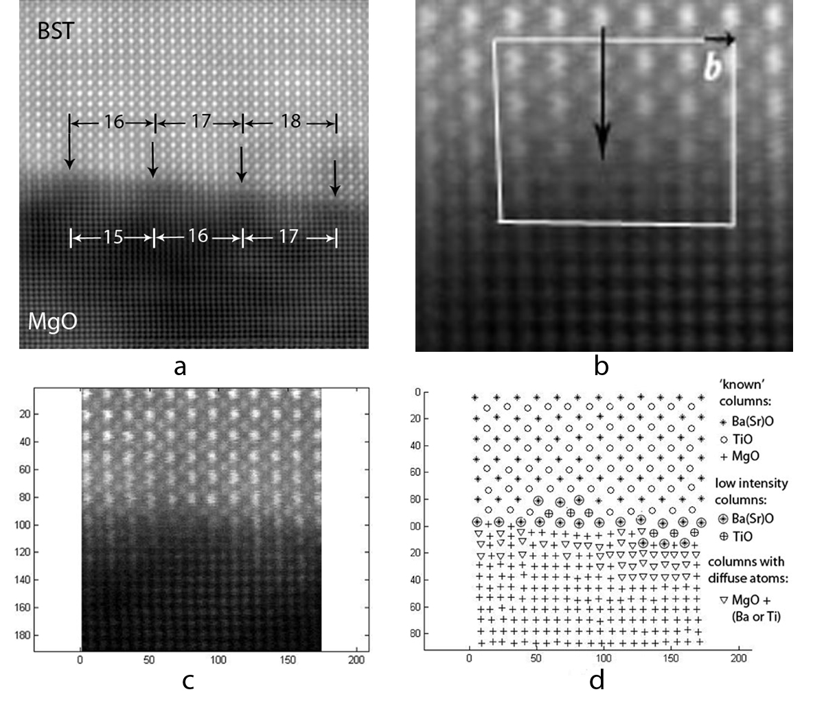
Fig. 1: HAADF STEM images of the 120 nm BST film. Misfit dislocations marked by arrows and numbers of half-planes between them (a), an enlarged part of the interface with one misfit dislocation and its Burgers vector (b),an enlarged part of the interface and corresponding map with estimated scattered intensities (c) and (d), respectively |