IT-9-P-2034 Imaging of grain boundaries in polycrystalline samples by HRTEM
Simultaneous imaging of neighboring grains and the grain boundary between them is tedious if polycrystalline samples are to be examined with random orientation distribution of submicron sized grains. The tilting range of HRTEMs is limited to about 20° and there is a low probability to find simultaneously resolved planes and especially low index zones for both grains within this tilting range by chance. Operation of a computer assisted method is demonstrated here that aids such imaging. The method is a combination of the commercial precession electron diffraction (PED) system [1] deployed on a JEOL 3010 with a new computer program that predicts tilt values needed for simultaneous HRTEM imaging of the grains selected from the orientation map.
The best scenario is when we are able to orient low index zones parallel to the electron beam in both grains and the grain boundary is also parallel to the beam simultaneously. A solution with compromise is if only one of the grains is seen from a low index zone while only one plane-set is resolved for the other.
Miller indices of the grain boundary plane in the coordinate systems of both grains are determined from its projection and the local thickness (or from projections at two tilt values as an alternative). The method also comprises the calibration of the directions of the tilt axes in the image.
The evaluation process can be applied to both cubic and non-cubic crystal systems and even to phase boundaries since the calculation of orientations and sample tilts is based on the general metric matrix formalism.
Application of the method is demonstrated here on hcp ZnO thin film with grain size of ca. 20‑40 nm deposited on Si substrate. Figure 1 shows the orientation map of the interested area. Different colors represent different orientations (blue area at bottom is the Si substrate) therefore individual grains can be recognized. The chosen boundary is marked by the white arrow. Figure 2 shows BF image of the layer while Figure 3 presents the HRTEM image of the observed boundary. The area marked by the dashed rectangle indicates a region where the two grains do not overlap, so the boundary is almost in the beam direction here. Fast Fourier transforms of the two grains, shown as inserts, corroborate that both grains are seen from the predicted orientations.
[1] J.Portillo, E.F.Rauch, S.Nicolopoulos, M.Gemmi, D.Bultreys: Precession Electron Diffraction assisted Orientation Mapping in the Transmission Electron Microscope, Materials Science Forum Vol. 644 (2010) pp 1-7 doi: 10.4028/www.scientific.net/MSF.644.1
Z. Baji is acknowledged for the preparation of the ZnO layer by ALD.
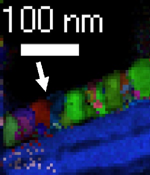
Fig. 1: Orientation map; probe size: 10 nm, step size: 5 nm. The observed boundary is marked by the white arrow. |
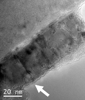
Fig. 2: Bright field image taken at the area of interest. The observed boundary is marked by the white arrow. |
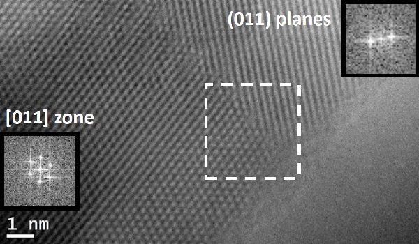
Fig. 3: High resolution image of the neighboring grains showing the first grain from [011] i.e. [-1 2 -1 3] zone. The (011) i.e. (0 1 -1 1) planes are only resolved for the second grain. The selected area shows the best insight into the structure of the boundary. |
|