IT-5-O-2005 Electron energy losses and cathodoluminescence from complex plasmonic nanostructures : spectra, maps and CL radiation patterns from a generalized field propagator
Stimulated by both instrumental (monochromators, detectors) and methodological (signal deconvolution and processing) advances, fast electron based spectroscopies have demonstrated their unique potential in probing surface plasmons (SP) of metallic nanostructures. Their nanometer spatial resolution and ability to probe so-called dark modes have given Electron Energy Loss Spectroscopy (EELS) and Cathodoluminescence spectroscopy (CL) a central role in experimental nano-optics. Today, these techniques are used to investigate nanostructures of increasing complexity in which the particle morphology, the substrate, or the interparticle interactions strongly influence their optical response[1]. Several examples of recent breakthroughs in combined electron/optical spectroscopy techniques such as Electron Energy Gain Spectroscopy demonstrated in ultrafast Transmission Electron Microscopes or surface plasmon three-dimensional imaging push forward the need and development of novel simulation techniques. In this context, we have developed a novel simulation technique allowing to describe thoroughly the interaction of fast electrons with metallic nanostructures. Building on the 3D Green Dyadic Method, our technique yields accurate predictions of the energy losses and CL photon emission consecutive to the interaction of a moving charge with a metallic nanostructure. It can be applied to nanostructures of arbitrary morphology, both penetrating and non-penetrating trajectories and rigorously takes into account the dielectric response of the substrate. Several examples will be presented which show an excellent agreement with recent experimental results. The influence of the substrate on the EELS spectra will be addressed. EELS spectra and maps (Fig. 1), CL spectra, maps and radiation patterns (Fig. 2) of several gold nanostructures from well-known textbook examples (nanoprisms, rods...) to more complex architectures (nanoporous films, particle aggregates, Fig. 3-4) will be presented. Finally, the potential of our technique will be illustrated on complex scenarii involving electron/photon interactions.
The authors acknowledge financial support from the European Union under the Seventh Framework Programme under a contract for an Integrated Infrastructure Initiative Reference 312483-ESTEEM2 and the National Research Agency under the program ANR HYNNA (ANR-10-BLAN-1016)
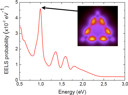
Fig. 1: EELS spectra computed at 9 nm from a gold nanoprism edge (edge length a = 950 nm, thickness t = 15 nm lying on a Si3N4 substrate (εsub = 3.9). The electron kinetic energy is 200 keV. Inset: EELS maps computed at 1 eV. The EELS probability is per electron and per unit energy. |
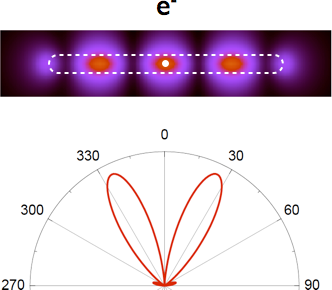
Fig. 2: Above: CL intensity per electron per unit energy range at 1.42 eV induced by a 200 kV electron incident on a gold nanowire (length L=700 nm, diameter D = 50 nm) deposited on a substrate with εsub = 4. The collecting mirror has a numerical aperture NA = 0.8. Below: CL radiation pattern for an electron incident at the center of the nanowire. |

Fig. 3: Randomly generated nanostructure composed of 29 gold spheres (diameter D = 9 nm). The particles are on a glass substrate (εsub = 2.25). |
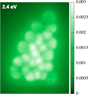
Fig. 4: Corresponding computed EELS probability maps for a 200 kV electron incident computed at 2 eV. |