IT-7-O-1998 In situ STEM studies of reversible electromigration in thin palladium–platinum nanobridges
Electromigration is a process in which a metallic contact line is thinned by passing a current through it, thus gradually displacing atoms and ultimately leading to its destruction [1]. The electromigration process in Pd–Pt nanobridges was investigated by in situ scanning transmission electron microscopy (STEM), using a FEI Titan operating at 300 keV. This technique together with a special electrical sample holder, built in-house, allows the nanobridge morphology transformations to be imaged down to the atomic scale during passage of electrical current [2]. Correspondent I–V curves are also recorded in real time. We focus in particular on the direction of material migration in relation to the electric current direction.
Polycrystalline Pd–Pt nanobridges with different lengths (500–1000 nm) and widths (200–500 nm), and a thickness of 15 nm were produced by e-beam evaporation from a metal alloy source onto a 100-nm-thick freestanding silicon nitride membrane [3] (Fig. 1a). The experiments were conducted in bias-ramping mode, i.e. a uniform increase in voltage from 0 V to a maximum of 350–600 mV (this was chosen in each separate experiment), followed by a decrease back to 0 V, sometimes a subsequent increase into the negative range (−350 to −600 mV) was done, followed by a decrease back to the original starting point of 0 V (Fig.1b).
Electromigration in Pd–Pt alloy [4] is quite different from the pure elements Pt and Pd. Material transport in Pt and Pd is very similar: after a recrystallization (which resembles that of the Pd–Pt alloy) the bridge gradually becomes narrower until a nanogap is formed, whereby grain boundary grooving is not a dominant feature. For the Pd–Pt alloy the dominant change is grain boundary grooving (which occurs near the cathode side), where the outer shape of the nanobridge is maintained. For high current densities (3 – 5×10⁷ A/cm2), material transport in Pd–Pt alloy occurs from the cathode towards the anode side, indicating a negative effective charge. While polarity is changed, the voids formed near cathode side are refilled (Fig. 2). The reversal of material transport upon a change of the electric field direction could be the basis of a memristor.
[1] Ho, P. S.; Kwok, T. Rep Prog Phys 1989, 52, (3), 301-348.
[2] Rudneva, M.; Kozlova, T.; Zandbergen, H. Ultramicroscopy 2013, 134, 155-159.
[3] Gao, B.; Osorio, E. A.; Gaven, K. B.; van der Zant, H. S. J. Nanotechnology 2009, 20, (41), 415207.
[4] Kozlova, T.; Rudneva, M.; Zandbergen, H. Nanotechnology 2013, 24, 505708.
The authors gratefully acknowledge NIMIC and ERC project 267922 for support.
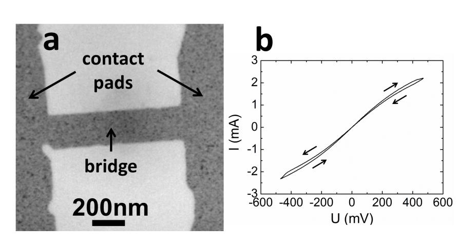
Fig. 1: (a) Typical TEM image of the initial configuration of the bridge. (b) Typical I–V curve for one loop in bias ramping mode. |
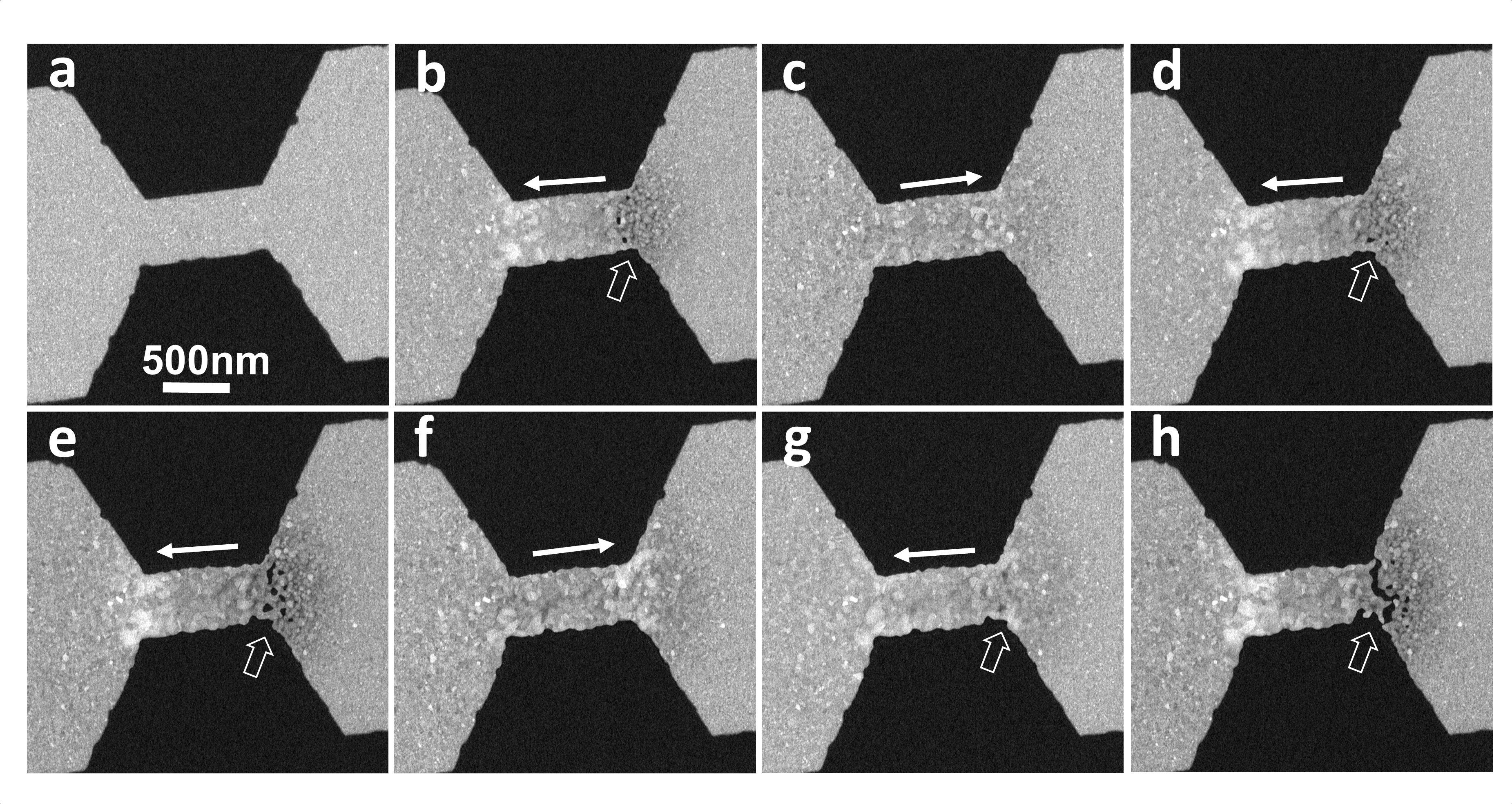
Fig. 2: Snapshots from the STEM footage. (a) Initial view of the bridge. During electromigration, voids form on the cathode side (shown with wide arrow) and material accumulates on the anode size (b, d–e, g–h). When the current is reversed, the voids are refilled (c, f). White arrows indicate the direction of electrons. |