IT-5-P-1978 Plasmon and dielectric function mapping of multiple InGaN QW sample by HAADF-EELS.
A thorough examination of InGaN quantum wells (QWs) was carried out through high angle annular dark field (HAADF) and electron energy loss spectroscopy (EELS) by aberration corrected scanning electron microscopy (STEM). The considered nanostructure consists of ~1.25 nm QWs layers with 20% indium content, periodically distributed along ~6 nm InGaN barriers, with 5 % indium content.
High resolution HAADF images give structural information from the examined crystal lattice below the nanometer range. Z-contrast in these images reveals the position of the QWs, the occurrence of In diffusion or even the formation of In-rich islands. Moreover, this information can be exploited using geometric phase analysis (GPA) algorithms in order to obtain maps of the deformation along lattice directions. The resulting deformation maps reveal that the structure suffers a localized distortion along the growth axis related to the In-rich QW positions (see Fig. 1).
STEM-EELS spectrum images (SI) are used to gain insight into the material properties of the sample. For this purpose, maps of plasmon peak energy and width are obtained and compared with the HAADF images. Generally, for III-V materials, compositional information can be recovered from the analysis of the plasmon peak energy through Vegard law [1]. In the present case, the small size of the examined QW and plasmon delocalization make this approach difficult to apply. However, the analysis of the plasmon witdth reveals a consistent swelling of the peak related with the position of In-rich regions, along with some expected shift to higher energy (see Fig. 2).
Furthermore, Kramers-Kronig analysis (KKA) of the EELS allows recovering the complex dielectric function (CDF) which contains electro-optical information from the material. For instance, it is possible to calculate the electron effective mass (m*) from the recovered CDFs at each pixel of the EELS-SI. The obtained values of m*, ranging from 0.14·m0 to 0.18·m0 are among the expected for InGaN (m*GaN = 0.2·m0 m*InGaN=0.11·m0). Moreover, depression regions in which the m* values are consistenty lowered are found in regions related with the ones having wider plasmon peaks (see Fig. 3).
All the computational work has been performed using the Hyperspy toolbox. The collection of techniques that have been developed in order to perform these analyses, will be presented along with the obtained results.
[1] A. Eljarrat et al. (2012) Microsc. Microanal. 18, 1143-1154.
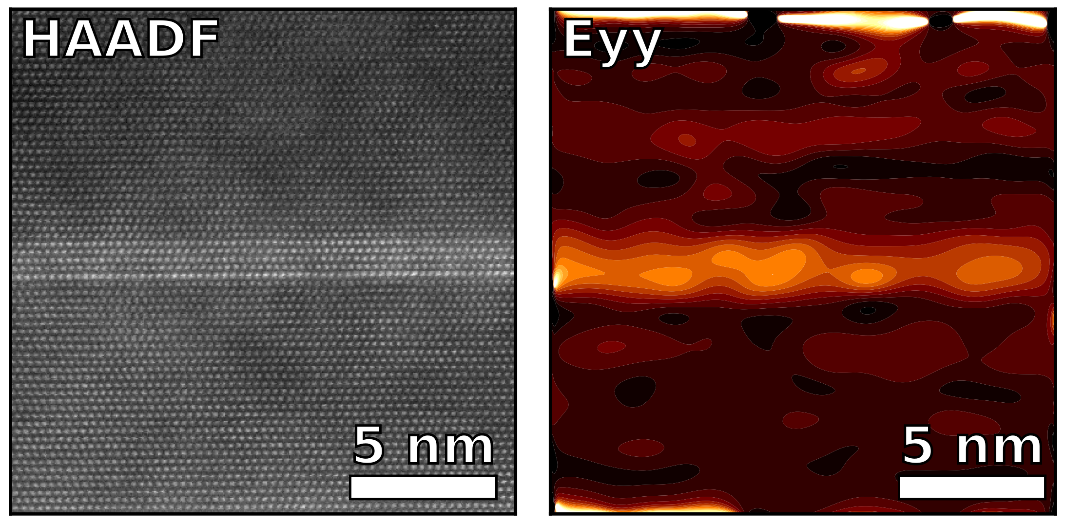
Fig. 1: Left panel, HAADF-STEM image of the structure, revealing the position and width of an In-rich QW. Right panel, deformation in the growth direction calculated from the previous image by GPA. |
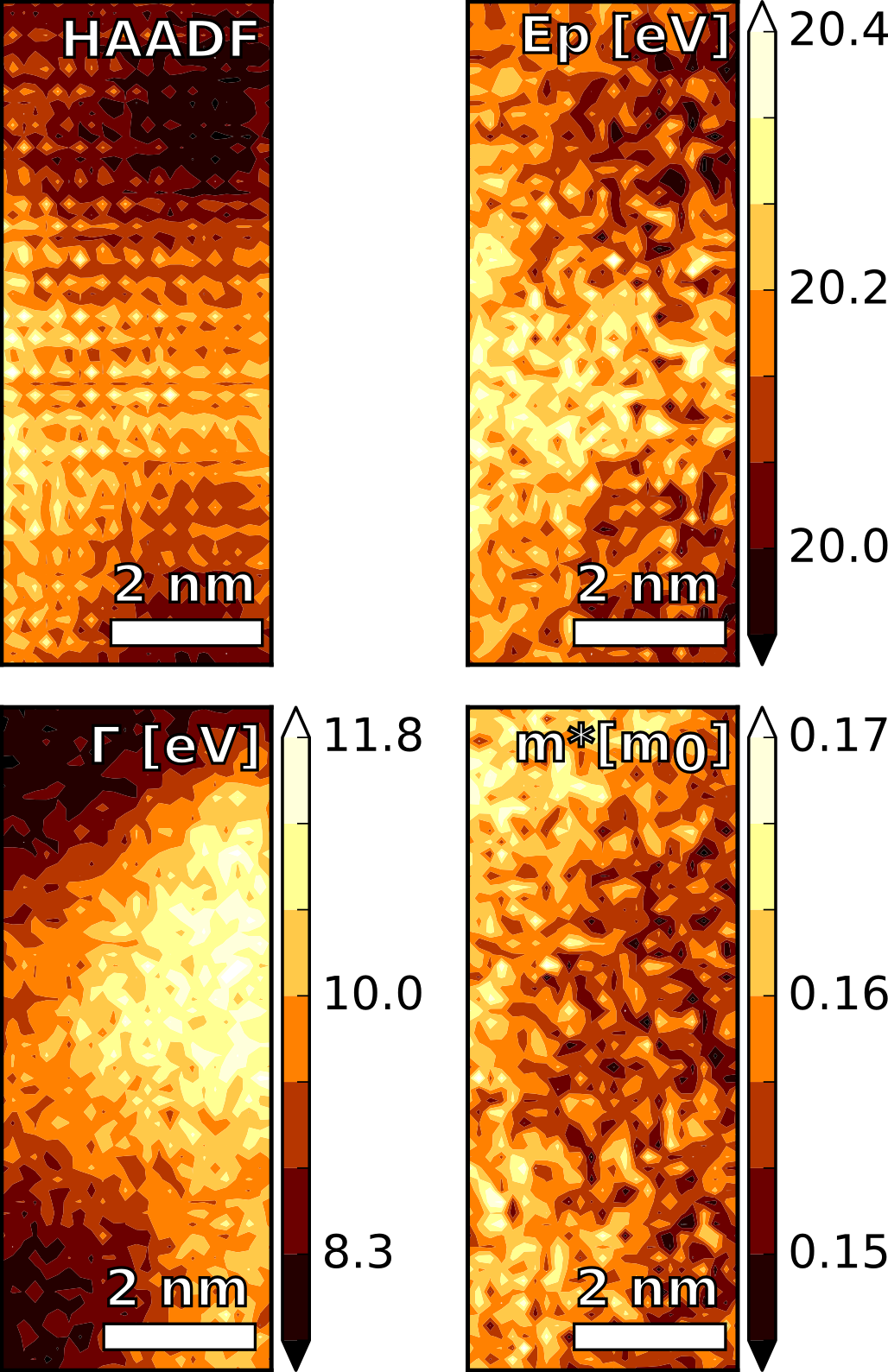
Fig. 2: HAADF image and results from the analysis of the simultaneously acquired EELS-SI on an In-rich QW region. The plasmon analysis reveals a shift towards higher energies (Ep) and a swelling (Γ) of the plasmon peak around the QW. The effective mass (m*) shows a characteristic depression around the same region as the swelling in Γ. |
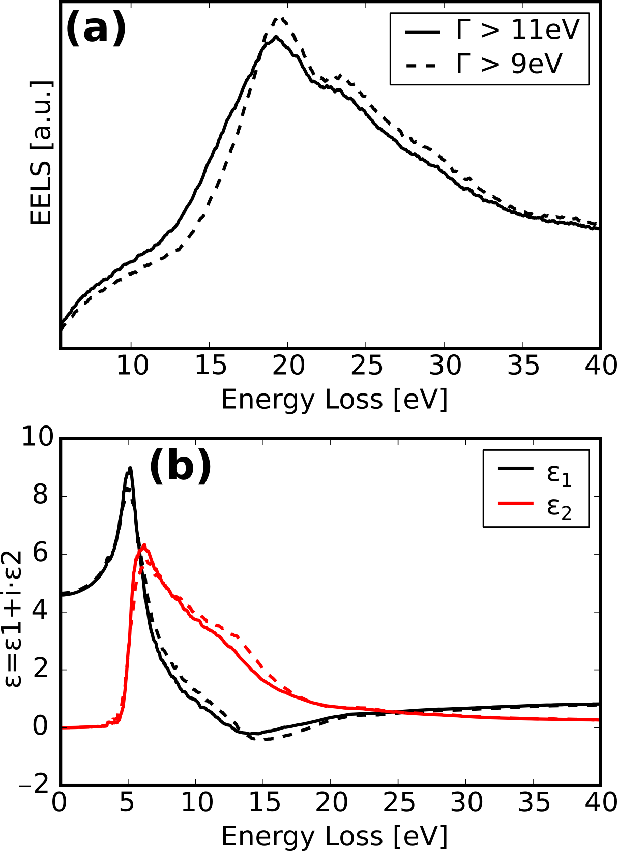
Fig. 3: The upper panel shows two average EELS in the narrow Γ (dashed line) and wide Γ (solid line) regimes. Also following this line code, the lower panel shows the real (red) and imaginary (black) parts of the average CDF from these same regions. |
|