IT-11-P-1945 Dopant mapping in thin FIB prepared silicon samples by off-axis electron holography
Modern semiconductor devices function due to accurate dopant distribution. Off-axis electron holography (OAEH) in the transmission electron microscope (TEM) can map quantitatively the electrostatic potential in semiconductors with high spatial resolution. For the microelectronics industry, ongoing reduction of device dimensions, 3D device geometry, and failure analysis of specific devices require preparation of thin TEM samples, under 70 nm thick, by focused ion beam (FIB). Such thicknesses, which are considerably thinner than the values reported to date in the literature, are challenging due to FIB induced damage and surface depletion effects.
We report1 on preparation of TEM samples of silicon PN junctions in the FIB completed by low-energy (5 keV) ion milling, which reduced amorphization of the silicon to 10 nm thick. Additional perpendicular FIB sectioning (e.g. Fig. 1) enabled a direct measurement of the TEM sample thickness in order to determine accurately the crystalline thickness of the sample. Consequently, we find that the low-energy milling also resulted in a negligible thickness of electrically inactive regions, approximately 4 nm thick. The influence of TEM sample thickness, FIB induced damage and doping concentrations on the accuracy of the OAEH measurements were examined by comparison to secondary ion mass spectrometry measurements as well as to 1D and 3D simulations of the electrostatic potentials. We conclude that for TEM samples down to 100nm thick, OAEH measurements of Si-based PN junctions, for the doping levels examined here, resulted in quantitative mapping of potential variations, within ~0.1V. For thinner TEM samples, down to 20nm thick, mapping of potential variations is qualitative, due to a reduced accuracy of ~0.3V (Fig. 2).
1. A. Pantzer et al., Ultramicroscopy 138 (2014) 36–45
We thank A. Ripp for advising and implanting PN junction samples; M. Sokolovsky for SIMS analysis; I. Amit and Y. Rosenwaks for assistance with ‘Sentaurus’ 3D simulator.
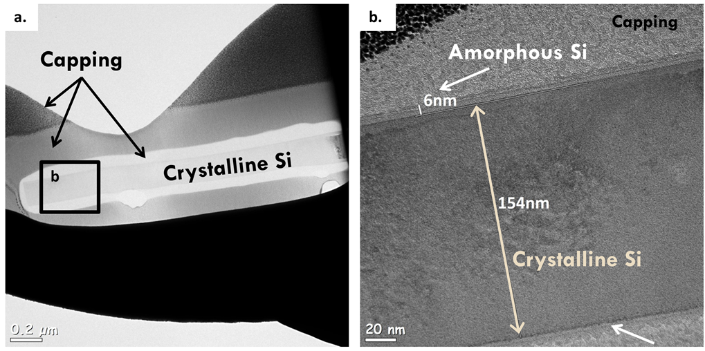
Fig. 1: Example (50 nm thick sample) of additional perpendicular FIB sectioning to measure layer thicknesses directly: (a) bright-field TEM overview image of the sample; (b) High-resolution TEM image of the region denoted schematically by the black rectangle in (a). A 6 nm thick amorphous Si surface layer is measured and 154 nm thick crystalline Si layer. |
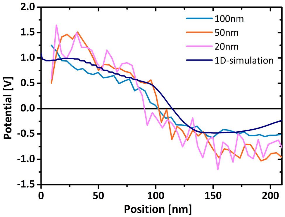
Fig. 2: Comparison of potential profiles for sample thicknesses varying between 20 and 100 nm as derived from OAEH to the band potential as calculated by a 1D Poisson simulation using data from SIMS measurements. |