IT-4-P-1865 Low-Damage SEM Imaging of Organosilicate Glass Thin Films in Semiconductor Industry
On-chip interconnect stacks of high-performance microelectronic products like microprocessors consist of Cu interconnects and insulating organosilicate glass (OSG). Dielectrics with extremely low dielectric permittivity (k value) are needed to reduce signal delay time and cross-talk in on-chip interconnects systems. The OSG thin films are either dense (so-called low-k materials) or porous (so-called ultra-low-k materials).
Imaging of dense and porous OSG thin films with Scanning Electron Microscopy (SEM) is necessary in semiconductor industry for process monitoring and physical failure analysis. Due to weak chemical bonding in the glass network, these materials show strong degradation effects when observed in SEM, caused by electron-material interaction. Particularly, the glass network is densified during the electron beam application to the sample, which phenomenologically causes a significant shrinkage of the material. This shrinkage avoids e. g. a quantitative determination of geometric features in semiconductor structures, which is required for process monitoring. Imaging with reduced primary beam energy mitigates the materials damage; however, the spatial resolution is usually reduced at lower accelerating voltages. In this study, spatial resolution and OSG thin film degradation during SEM imaging are studied systematically as a function of the primary beam energy. A Carl Zeiss SEM/FIB system NVision40 with Gemini column and three types of detectors is used, the conventional Everhart-Thornley detector, the inlense detector and the energy selective backscattering (EsB) detector. The optimum parameters for SEM imaging of OSG thin films are provided for several types of materials.
We kindly thank Carl Zeiss Microscopy GmbH for funding the investigations in the framework of the project “Untersuchungen zur Charakteristik und Applikation des EsB Detektors”.
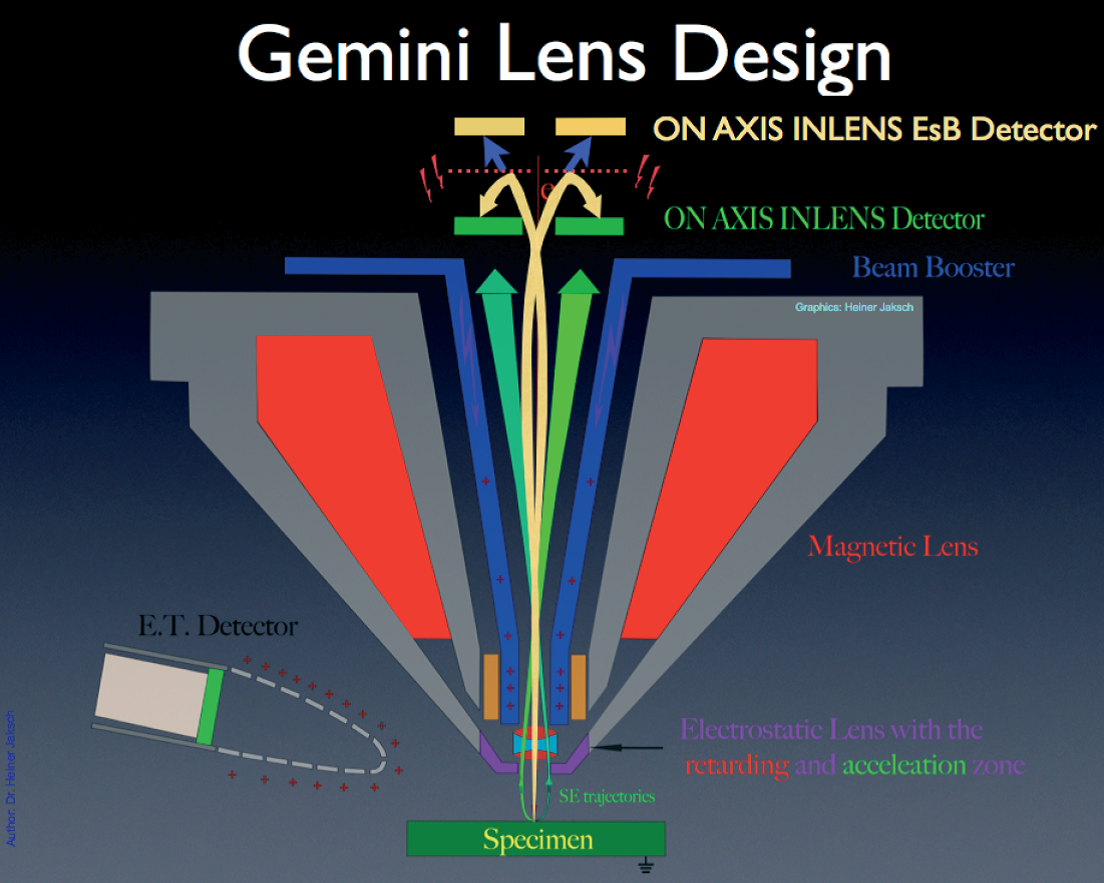
Fig. 1: Schematic of the Zeiss Gemini Column with three different electron detectors |
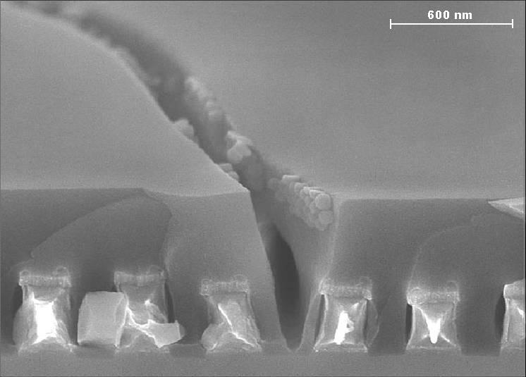
Fig. 2: Crack in low-k dielectric after one single scan in SEM |