IT-5-P-1842 Advanced SEM/EDS analysis using an Annular Silicon Drift Detector (SDD): Applications in Nano, Life, Earth and Planetary Sciences below Micrometer Scale
Analysis of fine-scale structures requires low accelerating voltages. Consequently, only low to intermediate energy X-ray lines with many peak overlaps can be evaluated which requires deconvolution. Examination of nano-scale structures also requires low probe currents which would give low X-ray count rates with traditional EDX detectors. The additional time required to acquire sufficient data for deconvolution risks altering the specimen as a result of beam-sample interaction or sample contamination. The BRUKER XFlash 5060F SDD has allowed us to overcome these limitations and offers additional benefits as we demonstrate here.
The annular SDD is inserted between the pole piece and sample and has a large solid angle (1.1sr). It is ideally suited for the analysis of topographically complex, three-dimensional samples. X-rays are collected from 4 separate detector segments and signals are processed in parallel by 4 detection units allowing high count rates at low dead-time. Even at lowest beam current (<10pA), samples can be investigated under high vacuum in natural state. In VP mode, sufficient statistics can be collected with reduced acquisition times, consequently reducing the likelihood of sample contamination.
4 studies are presented here. Experimental impact foil craters (Fig. 1) used to develop methodologies for the examination of samples from NASA’s STARDUST mission were examined (6kV, 1,100kcps, 45% dead time, 4096 x 3072 pixels, 62nm pixels, 7 min). Residues of glass projectiles can be clearly distinguished from the aluminium target with no detector shadowing across the field of view. Fig. 2 shows a portion of the Martian meteorite “Tissint”. This analysis was carried out at low beam current (4kV, <10pA, 733x853 pixels, 55nm pixels, 13 h). The mapped area revealed a thin coating and local enrichment of carbon (and nitrogen). The third study (Fig. 3) was carried out under low vacuum (20Pa, 5kV, 1.8nA, 20kcps, 320x240 pixels, 460nm pixels, 33 min) and shows mineralization in the ovipositor of a parasitoid wasp. Sufficient data quality allows deconvolution of overlapping element lines (Zn-L, Na-K). The final study (Fig. 4) demonstrates that the analysis of core-shell nano particles (5kV, 520pA, 14-72kcps, 250x250 pixel, 2nm pixels, 6 min) on thin film supports has become possible.
It can be concluded that improvements in SDD technology will stimulate new approaches for various fields. To minimize acquisition time and increase spectrum statistics, the total solid angle is relevant, not the active detector area. Element analysis at low kV and low beam current in combination with multi-segment SDDs provides high spatial resolution and high detection sensitivity without the necessity of applying a conductive coating or working in low vacuum.
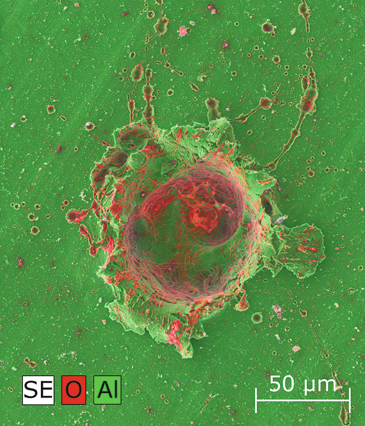
Fig. 1: Stardust analogue crater experiment; Composite EDX map overlain with SE micrograph reveals residues of glass projectiles (red) on an aluminium target (green). |
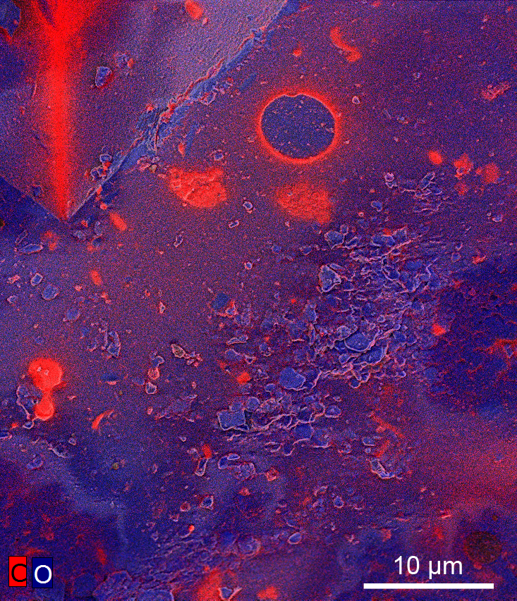
Fig. 2: Tissint Martian meteorite; Composite EDX map of carbon and oxygen overlain with SE micrograph shows a thin coating and local enrichment of carbon. |
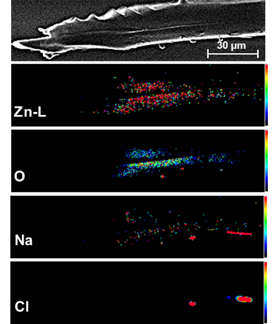
Fig. 3: Biomineralization in a parasitoid wasp Monolexis fuscicornis. The ovipositor (sting and egg-layer) reveals ZnO reinforcement and contamination with NaCl. |
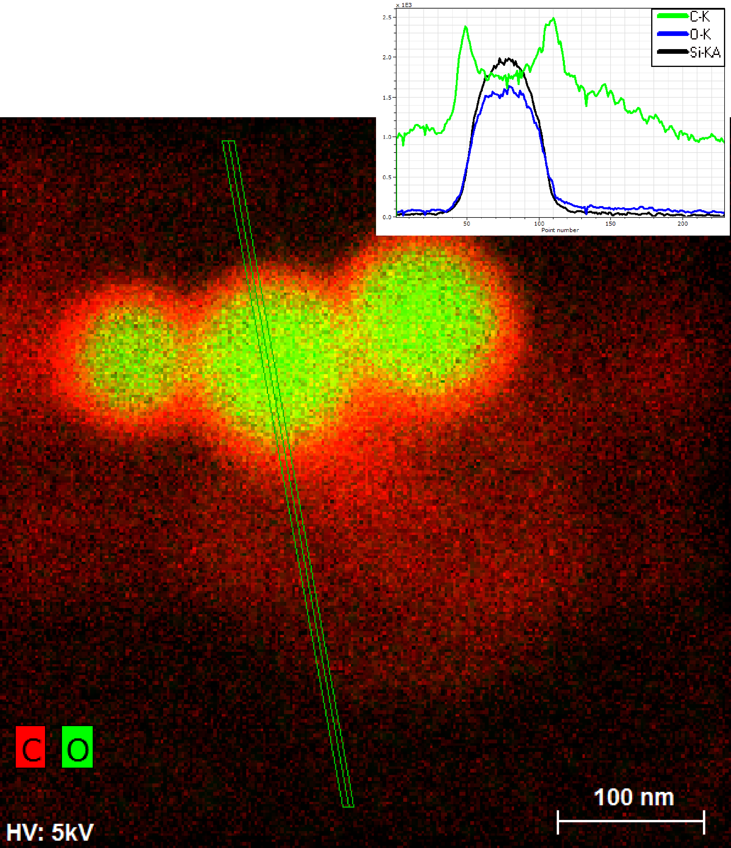
Fig. 4: Composite EDX map of fluorescent silica nano particles. At the line scan (net intensities, 229 points, 467nm length, 30kcps, and 6.9 s), five adjacent pixel/spectra were binned for each point in order to improve impulse statistics. |