IT-4-P-1829 Determination of the second critical energy of primary electrons in relation to dielectric thickness and angle of incidence
At the second crossover energy E2C of incident electrons the equilibrium is maintained between the electron probe currents I0, the second electron emission (SEE) currents I0δ, the backscattered electron (BSE) currents I0η, as well as the leakage currents IL and the displacement currents Id that are responsible for the accumulated charge Q. At the equilibrium state the equality I0=I0(δ+η)+IL+Id is fulfilled, while for the target remaining uncharged the condition δ+η=1, VS=0 is valid, where δ and η are the emission coefficients of SE and BSE.
Experimental results for dielectrics, in the case when incident electrons impinge on the sample surface at the angle α, can be described by the following semi-empirical expression: E2C=E2C(0)exp[(ln(R2C/2λ))(1-cosα)], (1)
where λ is the effective emission depth of SE, R2C=76E01,67 ρ is the depth of penetration of primary electrons with the energy E0, ρ is the specific density of the dielectric material. As an example, fig.1(a) shows the experimental dependence and the dependence calculated by formula (1) of the second critical electron energy E0=E2C on the angle of incidence α, for the target potential VS=0, i.e. when the target remains uncharged. Fig.1(b) shows the dependence of the energy E2C on the angle of incidence α for ungrounded metals.
Consider the dependences of the VS of PММА films with the thickness d on a silicon substrate at the electron energy E0.
The experimental results are in qualitative agreement with the calculated results as shown in fig.2(a), presenting the dependences VS(d) for MICA plates 2 to 30 μm thick and for PММА films 0.4, 1.4, 2.7, 4 μm thick on the Si-substrate.
At the radiation energies E0 in the range of 0.5–1.0 keV the negative charging begins (note that according to previous views, positive charging was expected because E0<E2C). At this energy the sign polarity of VS changes, i.e. at the point where VS=0 V. For PММА this value lies in the range E0=0.4–0.6 keV, with the thicknesses of the layers of positive and negative charges and the values of these charges are approximately equal (λ≈R0, Q+=Q-), which is responsible for the total absence of charging. In the region of 1 keV <E0<Ecr2 one can clearly observe negative charging, and the greater d, the higher the value of -VS. This range corresponds to the condition λ<R0<d. The value of -VS at first increases and reaches the maximum, then as E0 and R0 grow, it starts decreasing slowly in the absolute value and reaches zero at the points of Ecr2, that are different for each film thickness d. These points can be used in high-voltage lithography, because it is at these values of R0≥2d that the conduction current IT is generated and it carries excessive negative charges (electrons) onto the substrate, hence VS=0 V.
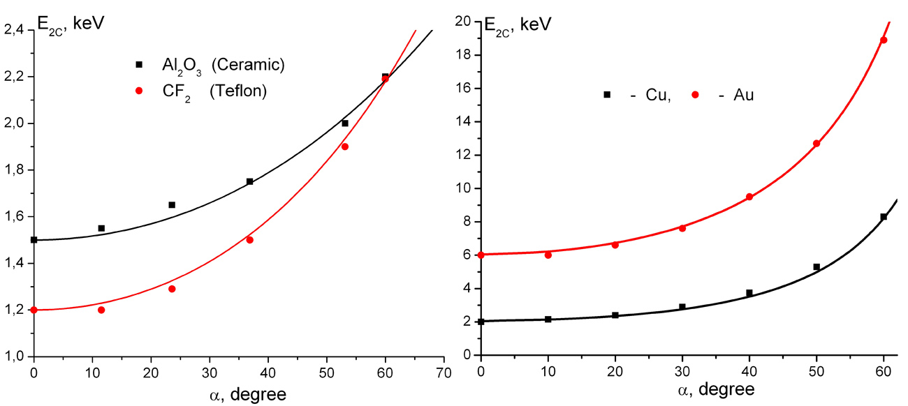
Fig. 1: Characteristics of the value of the second critical electron energy E2C as a function of angle of incidence α for dielectrics (a) and ungrounded metals (b). |
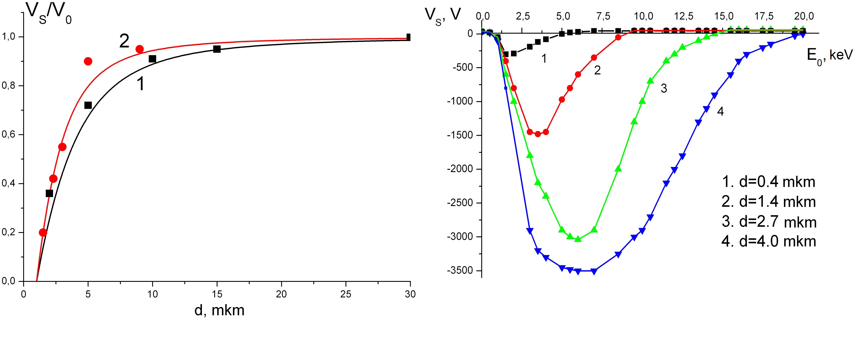
Fig. 2: (a) - Dependence of surface potential of dielectric films on their thicknesses: (1) VS(d) for mica (plot 1) and for PММА (plot 2). (b) - Dependences of surface potential VS on incident electron energy E0 for PММА films of different thickness d on Si-substrate. |