IT-4-P-1825 The study of extreme low landing voltage scanning electron microscopy
The development of low voltage (LV) FE-SEMs have been in progress, and spatial resolution better than 1 nm can now be achieved even at 1 kV. General LV FE-SEMs are available for a sample surface observation and low voltage EDS analysis. Furthermore, by choosing appropriate observation conditions, we can selectively obtain different information such as material topography and composition. In this report, authors focused on observations at extreme low impact electron-energy in order to obtain information from surface. For example, the length of electron mean free path at 100 eV in a solid sample is smaller than 1 nm [1]. So that it is expected to observe clearly surface morphology. Moreover, we can expect what the low impact electron energy show less electron beam damages in general [2].
Recently, we can use combined lens both electrostatic and magnetic to minimize Cc as well as field emission type emitter with high brightness [3]. So-called Super Hybrid Lens (SHL) is equipped on JSM-7800F. In addition, negative surface potential can be applied on the specimen surface by so-called Gentle Beam mode (GB). Therefore, the impact electron energy to the specimen surface can be reduced down on 10 eV keeping the probe size small with high coherency.
Figs.1 (a) and (b) show carbon nanotubes observed at 80 eV and 500 eV. Those images clearly show their shapes even at 80 eV. Fig.1 (a) shows less edge effect compared with (b) due to small penetration depth of electrons at lower impact electron energy. The intensity profiles along the lines shown in Figs.1 (a) and (b) are shown in Fig.1 (c). The 80 eV image shows higher contrast than the 500 eV one. We assume that is due to higher efficiency of interaction with carbon materials at lower impact electron energy.
Fig.2 (a) shows a low magnification image of meso-zeolite (LTA) at 80 eV. Figs.2 (b) and (c) show high magnification images at 80 eV and 500 eV. All images clearly show topological information at meso-LTA. Especially, the image of 80 eV shows less edge effect due to small interaction volume. That is a useful feature of LV FE-SEM because it can reveal fine edges and give high accurate measurement of nano porous materials. One other useful feature is the reduction of specimen damage due to electron irradiation. The gap shown between two arrows in a circle in Figs. 2 (b) and (c) is observed to be wider in the latter than in the former. The observation indicates less electron damage at 80 eV.
References:
[1] C. R. Brundle, J. Vac. Sci. Technol., 11, 212 (1974)
[2] L. Reimer, Scanning Electron Microscopy: Physics of Image Formation and Microanalysis, 2nd ed., Springer,
Berlin, New York, (1998)
[3] J. Frosien, J. Vac. Sci. Technol. B 7 (6), Nov/Dec (1989)
[4] O. Terasaki, JEOL News, (2013)
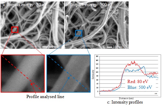
Fig. 1: Low impact electron energy on Carbon nanotubes |
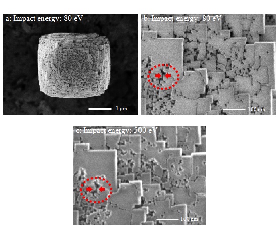
Fig. 2: Images of meso-zeolite (LTA) at two impact electron energy of 80 eV (a,b) and 500 eV (c). |