IT-7-P-1812 Dislocation mediated creep/relaxation in nanocrystalline palladium thin films revealed by on-chip high resolution TEM in-situ testing
The high rate sensitivity of nanostructured metallic materials demonstrated in recent literature is related to the predominance of thermally activated deformation mechanisms favoured by a high density of internal interfaces. In the present study, we report for the first time in-situ high resolution transmission electron microscopy (HRTEM) creep/relaxation tests on electron beam evaporated nanocrystalline (nc) palladium (Pd) thin films using an original on-chip nanotensile method resembling the technique used in [1]. Unexpectedly, large creep/relaxation rates have been observed at room temperature. Figure 1 shows the microstructure of the as-deposited Pd films characterized in both cross-sectional and plan-view thin foils prepared by focused ion beam (FIB). In this figure, columnar nanograins can be observed with 2 or 3 grains confined over the thickness of the films with an in-plane grain diameter of ~30 nm. Automated Crystallographic Orientation Mapping in TEM (ACOM-TEM) shows a clear [110] fibre texture parallel to the growth direction. The microstructure involves Σ3 60° {111} coherent twin boundaries (CTBs) in ~ 25% of the grains.
The in-situ HRTEM characterisation of the evolution of the microstructure shows that, despite the small grain size, the creep/relaxation mechanism is mainly mediated by the stress driven thermally activated nucleation and propagation of dislocations. Interestingly, the formation and the destruction of sessile Lomer-Cottrell dislocations have been observed in-situ. Furthermore, clear loss of the coherency of CTBs with time was observed as indicated by the progressive increase of the thickness of these boundaries as shown in Figure 2. Such feature is attributed to the interaction of CTBs with lattice dislocations. The impact of these elementary plasticity mechanisms on the creep/relaxation behaviour of the Pd films is discussed and compared to recent experimental and simulation works in the literature. This constitutes a key issue in the development of a variety of micro- and nanotechnologies, such as Pd membranes used in hydrogen applications.
References
1. H. Idrissi, B. Wang, M.S. Colla, J.P. Raskin, D. Schryvers and T. Pardoen, Adv. Mater. 23 (2011), P.2119.
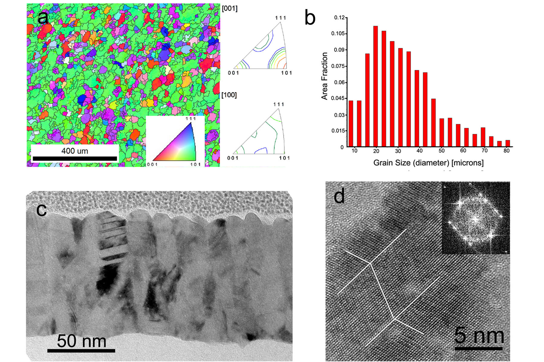
Fig. 1: Figure 1. a) ACOM-TEM orientation mapping of as-deposited Pd film. Corresponding inverse pole figure along different directions are shown. b) Grain size distribution of (a). (c) Bright field micrograph obtained on cross-sectional as-deposited Pd film (d) HRTEM image obtained in as-deposited films showing a Σ3 60° {111} coherent TBs. |
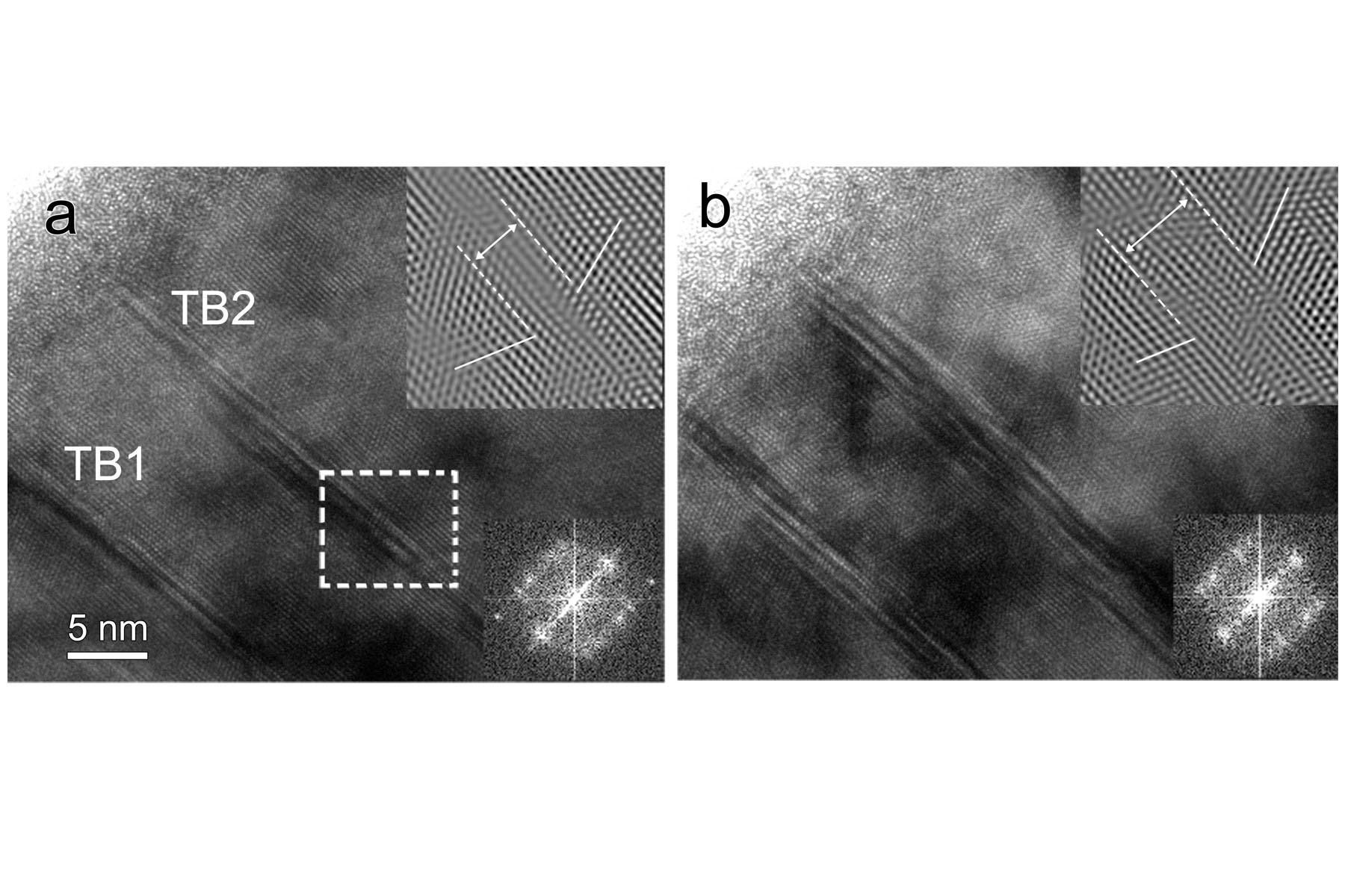
Fig. 2: Figure 2. HRTEM images showing Σ3 {111} TBs at (a) t=0 and (b) t=3 days, respectively. Note the increase of the TBs thickness from (a) to (b) in the filtered images at the upper right insets. Corresponding Fast Fourier Transform (FFT) showing the twin character is shown in the lower right inset of each image. |