IT-5-P-1811 Features and Applications of an Analysis System using Double Silicon Drift-type Detectors for Transmission Electron Microscopy
The elemental analysis using energy dispersive X-ray spectroscopy (EDS) requires considerably long time due to a small ionization cross section for core electrons of a specimen and a small solid angle for a detector. Therefore, the realization of an efficient, short time analysis not only serves the increasing needs of users but also reduces specimen damage due to electron irradiation. For this purpose, we have developed a new analysis system, which is extremely sensitive than the one at present. We report the features and applications of the newly developed analysis system, which is composed of two silicon drift-type detectors (SDDs).
Our newly developed analysis system consists of two SDDs (double-SDD) with a large sensor area (100 mm2 in area). Figure 1 shows the schematic configuration of the system for a field emission electron microscope (JEM-2800). A new TEM column has two ports for the detectors. And a special analytical specimen holder, which is thinner than the present one, has been newly developed to reduce the distance between the detector and specimen.
The total X-ray intensity of the new system has increased, because the X-ray signals collected from two detectors are integrated. The new specimen holder also promotes higher X-ray collection efficiency. As a result, total sensitivity has been significantly improved. For example, the peak intensity of Al K line obtained with a double-SDD has increased to be approximately 1.7 times higher than that obtained with a single SDD as shown in Fig. 2.
Since the new analysis system can provide high analytical sensitivity, an atomic resolution elemental map with a high S/N ratio can be acquired in combination with Cs-corrected TEM/STEM machines such as JEM-ARM200F. In the upper parts of Fig. 3 are shown atomic resolution elemental maps sized 128 x 128 pixels for SrTiO3<100>. These maps clearly show atomic columns of Sr, Ti and O. The profiles of elemental columns, displayed in the lower parts of Fig. 3, show a significantly improved signal to noise ratio for the double-SDD compared with the one for the single SDD.
Our new system has significantly high X-ray collection ability. Therefore, it provides a shorter acquisition time than a single SDD system. It helps us, beyond all doubt, to analyze a beam sensitive specimen and to detect trace elements in a specimen.
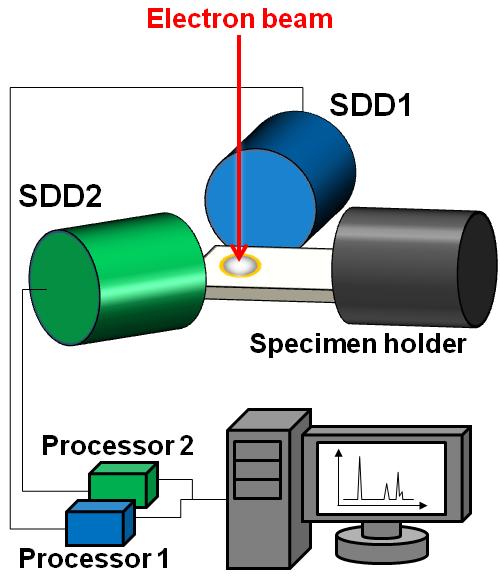
Fig. 1: Fig. 1: A schematic configuration of an EDS analysis system for a field emission electron microscope (JEM-2800). |

Fig. 2: Fig. 2: EDS spectra of an Al foil specimen, obtained by using JEM-2800 (200 kV) with SDD1+SDD2 (red) and SDD1 (blue), respectively. The vertical axis has been normalized by the peak intensity of Al K line, obtained with SDD1. |
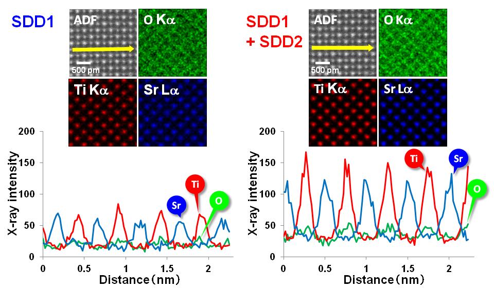
Fig. 3: Fig. 3: STEM-ADF images and atomic resolution elemental maps (O, Ti, Sr) for SrTiO3<100>, obtained with JEM-ARM200F (200 kV) with SDD1 (left) and SDD1+SDD2 (right). The mapping sizes are 128 x 128 pixels. Line profiles of O Kα, Ti Kα, and Sr Lα gross intensity extracted from yellow lines in ADF images are also shown below the maps. |
|