IT-4-P-1795 SEM images using an energy/angle selective electron detector.
Scanning electron microscopes (SEMs) are usually equipped with two types of detectors: secondary and backscattered electron detectors. The former produces secondary electron images (SEI) rich in topographic information[1, 2], whereas the latter produces backscattered electron images (BEI) rich in composition information[3]. Recently, however, a few other detectors have been installed in addition to these two types of conventional detectors[4]. In these practical detectors, however, it is difficult to see directly the effect of energy and take-off angle of the emitted electrons on the image contrast. In this study, an electron detector was designed and experimentally manufactured to detect electrons emitted in a definite, variable range of energy and take-off angle.
Figure 1 shows a schematic diagram of the newly designed electron detector, the E-θ detector, which can detect electrons emitted from a sample with a selected range of energy and take-off angle. The E-θ detector consists of a slit plate, inner and outer electrodes in a cage, and electron detectors. The slit plate is placed at a lower part of the E-θ detector. It serves as a selector of take-off angle. The range of take-off angle is selected mechanically by sliding the slit plate as shown in Fig. 1 and is measured from the horizontal direction parallel to the sample surface. The selection of electron energy is made by applying voltage to the inner and outer electrodes in the cage in accordance with electron take-off angles. In the case of the low angle range, positive and negative voltages are applied to the inner and outer electrode, respectively, as shown in Fig. 1(A), so that electrons are deflected towards the inside with the increasing amount of deflection with decreasing energy. In the case of the high angle range, the polarity of the applied voltage is reversed as shown in Fig. 1(B), so that electrons are deflected towards the outside. To enhance the electron detection, a metal mesh is placed in front of the electron detectors and a voltage of 2 keV is applied between the detectors and the metal mesh. When a series of concentric ring electron detectors with different diameters are placed at the upper part of the cage, each ring detector can collect electrons with a specific range of energy determined by the voltage applied to the two electrodes. As a preliminary study, we acquired images using commercial Si-photodiode (SiPD) as the electron detectors, as shown in Fig. 2.
[1] M. Kotera et al., Scanning Microscopy Supplement 4 (1990) p. 111.
[2] Y. Lin, D. C. Joy, Surface and Interface Analysis 37 (2005) p. 895.
[3] M. D. Ball, D. G. McCartney, Journal of Microscopy 124 (1981) p. 57.
[4] S. Asahina et al., Microscopy and Analysis, Nanotechnology supplement November (2012)
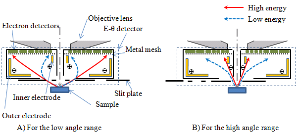
Fig. 1: Schematic diagram of the E-θ detector. |
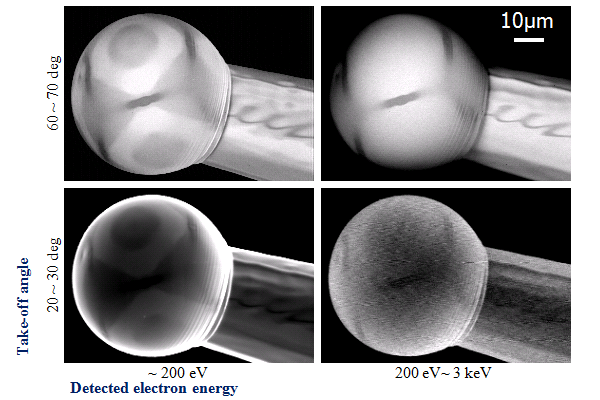
Fig. 2: SEM images acquired with the E-θ detector. The sample is a spherical single crystal of tungsten. |