IT-5-O-1775 Study of layer by layer graphitization of 4H-SiC, through atomic-EELS at low energy
Epitaxial graphene (EG) grown on Si-polarized SiC, play a crucial role by the presence of a so-called carbon “buffer layer”. Such layer has been shown to present a certain degree of sp3 hybridization since it is partially bound to the outmost Si atoms of the SiC (0001) surface [1].
Our results indicate a layer by layer graphitisation of the SiC as the Si evaporates. Atomic resolution EELS measurements show that the relative Si concentration across the buffer layer [2]. Moreover, the presence of oxygen has been revealed across the buffer layer as shown in Figure 1b. The presence of oxygen could be responsible of the slower decomposition of the SiC into graphitic layers. This and other aspects will be discussed.
All the STEM and atomic EELS measurements were performed at 60k. This consists of a probe corrected STEM microscope, capable to deliver a probe size of 1.1 Å, and equipped with a C-FEG and a fully loaded GIF Quantum ER as EELS spectrometer. Low- and core-loss spectra were nearly simultaneously acquired using the DualEELS capability. In this way an accurate measurement of the π*/σ* peaks ratio that is proportional to the sp2 contribution can be carried out. Low- and core-loss EELS spectra were taken across the green box in the ADF STEM image in Figure 1a using a pixel step size of 0.6Å and an exposure time of 20 ms for each pixel. The spectrometer was set to 0.25eV dispersion yielding 0.75eV energy resolution. Such energy resolution is sufficient to reveal different features in the fine structure of the C K-edge and Si L2,3-edges. The ADF STEM image in Figure 1a shows the presence of the buffer layer between the SiC substrate and the 3 graphitic layers. EELS spectra of the O K-edge, Si L2,3-edges and C K-edge are shown in Figures 1b,c,d respectively and were extracted from the selected positions in the sample as shown in Figure 1a. In Figure 1b, the O K-edge peak shows up only in regions 4 - 6 and is particularly strong in region 6. There seems to be in this region of the buffer layer an increase of the oxygen concentration. No oxygen is detected in either the SiC substrate or the graphitic layers. Particularly interesting are the C K-edge spectra in Figure 1d. The spectra in positions 1-3 in the SiC substrate region show different π* peak, indicating chemistry changes. The spectra extracted from the graphene layers in positions 7,8,9 show much higher contribution in the π* peak that leads to the fully sp2 hybridization indicating transition to graphitic structure. [1] G Nicotra et al, ACS Nano 7 (4), (2013) p. 3045.2 [2] G Nicotra et al, to be published
This work was performed at Beyondnano CNR-IMM, which is supported by the Italian Ministry of Education and Research (MIUR) under project Beyond-Nano (PON a3_00363); The SuperSTEM Laboratory is supported by the U.K. Engineering and Physical Sciences Research Council (EPSRC)
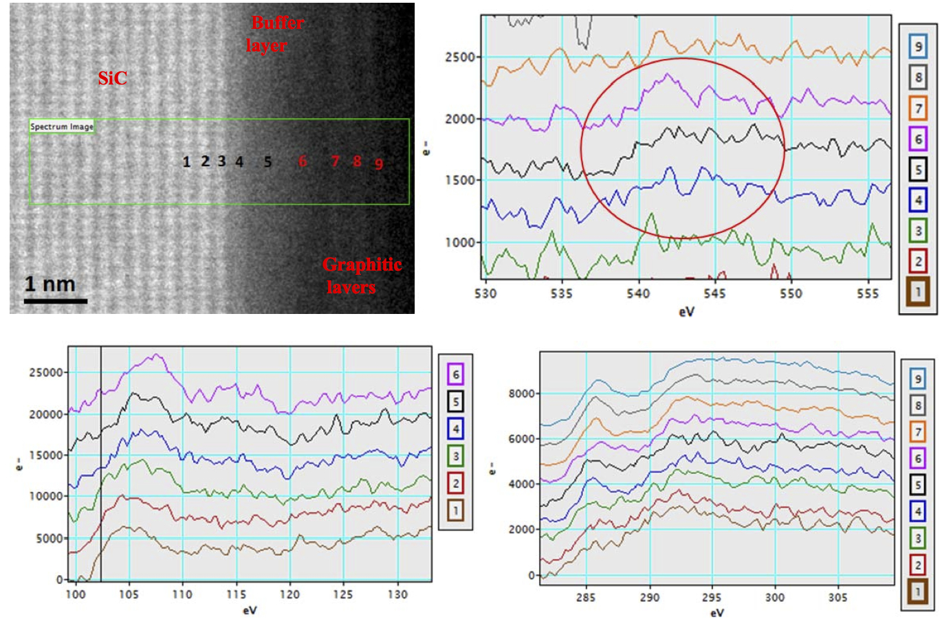
Fig. 1: a) ADTE STEM survey image. b-d) EELS spectra extracted from the selected positions in Figure 1a each spectrum was corrected for the effects of energy drift and plural scattering; b) O K at 532 eV slightly enlarged for better visualization; c) Si L2,3-edges at 99 eV; d) C K-edge at 284eV. Spectra from positions 7 – 9 are from the graphitic layers. |