IT-9-P-1694 Strain mapping at the nanoscale using precession electron diffraction in a non-corrected Transmission Electron Microscope
The electron precession [1] technique is a recent innovation in electron crystallography. The advantage of this technique is to minimize the dynamical effect to such an extent that diffraction images can be analyzed using a kinematical approach with minimal user intervention. As a first step we have performed Precession Electron Diffraction (PED) strain measurement on a simple calibration sample paving the way to the strain analysis on more complex devices from micro-electronic.
PED measurements were made using a JEOL-JEM2010FEF non corrected microscope operating at 200 kV. Precession beam scan alignment is performed employing NanoMEGAS’s “DigiSTAR” add-on device. Precession semi-angle was set to 1.44° to take full advantage of PED kinematical behavior. With a probe size as small as 4.2 nm FWHM is obtained on the sample with a convergence of 1 mrad.
The sample we have used is prepared from materials grown by RPCVD on a [001] Si Substrate. It is composed of four 10 nm SiGe layers with different contents in Ge separated by 30 nm of Si and covered with 150 nm Si capping layer. A 8 kV FIB operating voltage was used to provide 50 nm thin parallel-sided lamellae with reduced surface damage. This sample was specifically designed to benchmark strain studies [2] as it is easy to simulate the strain expected in TEM.
PED are recorded every 2.7 nm in a 185 nm x 240 nm region indicated in Fig. 2. using a 512 x 512 pixels Camera deported from the microscope optical axis. Classical projective geometry was used to correct most of distortions in misaligned cameras. Figure 1 (a) illustrates typical diffractions patterns acquired during experiments. Beam probe images were made with a CCD camera (Fig. 1) able to deal with high brilliance scenes and dedicated software was designed to compute PED patterns for strain analysis. The algorithm used takes advantage of the whole “kinematic” region in reciprocal space. The basis of vectors inherent in that periodic region is found using Delaunay triangulation and introduced in a reciprocal matrix G. From this matrix, the distortion matrix D can be retrieved, giving access to the strain ε matrix and rotation Ω matrix.
Figure 2 shows εxx strain mapping obtained by analysing the acquired diffractions patterns set with this method. The noise in 800 contiguous εxx values far from SiGe layers is rather small so that an rms of 3 10-4 is obtained. Strain profiles (Fig. 3) reveal the strong repeatability in measures. Both of them agree very well with finite element COMSOL simulation of the strain averaged along the beam direction and convoluted with the measured electron beam shape.
[1] Vincent, R., et al. « Ultramicroscopy, 53, 3,1994
[2] Rouviere, et al. Applied Physics Letters 103, 24,2013
This study was made possible through funding provided by ANR LABEX MINOS and ANR AMOS programs. Experiments have been done within the Nanocharacterisation Platform of the CEA/Grenoble, MINATEC Campus.
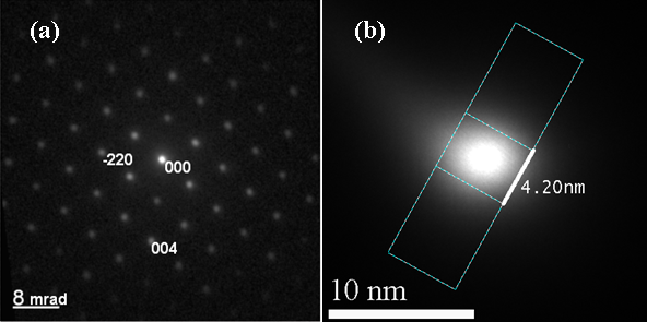
Fig. 1: (a) [110] PED diffraction patterns obtained in Silicon with the probe displays in (b). (a) 4.2 nm full width at half maximum spot size in silicon measured on CCD camera with 1.44° Precession semi-angle. |
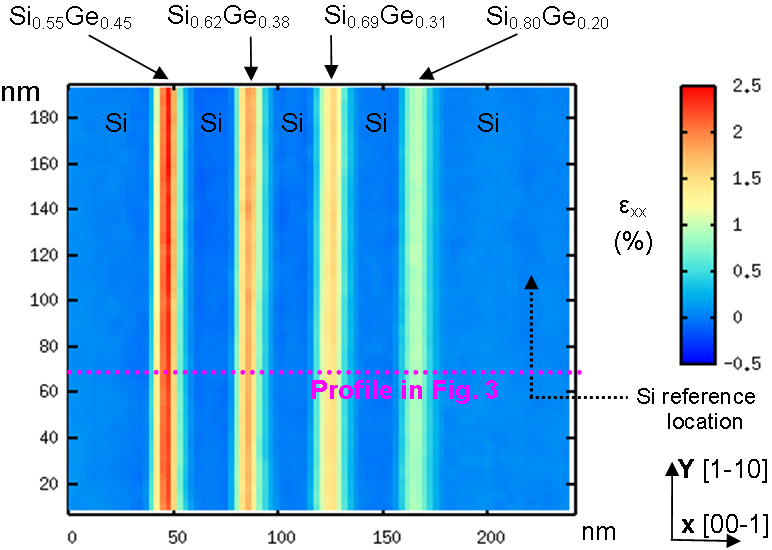
Fig. 2: SiGe Strain mapping with Precession (semi-angle set to 1.44°) |
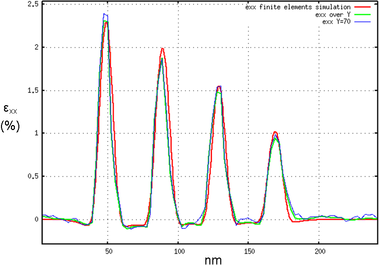
Fig. 3: εxx SiGe Strain profile along y=70 profile shown Fig. 3; mean εxx strain profile all over y; εxx SiGe Strain profile obtained by finite element COMSOL simulation. |
|