IT-5-IN-1656 Single atom imaging and spectroscopy with aberration-corrected STEM
Aberration-corrected scanning transmission electron microscopy (STEM) at low voltage can now provide real space imaging and spectroscopy measurements at the atomic scale with single atom sensitivity. This opens new opportunities for quantitative study of structural defects in 2D materials. Such studies, especially when combined with first-principles calculations, serve as an important step to correlate the defect structure with local properties, and help to create new functionalities in 2D materials via controlled defect engineering.
Figure 1 shows an experimental annular dark field (ADF) image of Se-doped MoS2 monolayer. Quantitative image analysis allows us to identify the chemical nature of the dopant and map out their distribution in MoS2, one atomic-layer at a time, providing a feasible way to quantify the local composition and measure the local band gap at the 10 nm scale [1].
Combining the imaging and spectroscopy power on a STEM, the changes in local optical response and electronic structure can be directly measured at defect sites. We show that the presence of a single Si atom in the graphene lattice can enhance the low-energy interband transitions with sub-nm spatial confinement [2]. Furthermore, the fine structure in electron energy loss spectra acquired under optimized dose levels provides the sensitivity to determine the nature of the chemical bonding of single atoms. We show that three-dimensional and planar bonding configurations for individual Si atoms in graphene can be directly discriminated (Figure 2) [3].
[1] Y. Gong et al., Nano Lett., 14, 442-449 (2014).
[2] W. Zhou et al., Nat. Nanotech., 7, 161-165 (2012).
[3] W. Zhou et al., Phys. Rev. Lett., 109, 206803 (2012).
This research was supported by a Wigner Fellowship of Oak Ridge National Laboratory (ORNL), the U.S. DOE Basic Energy Sciences, and ORNL’s Center for Nanophase Materials Sciences.
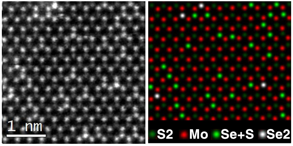
Fig. 1: Atom-by-atom Se dopant analysis in monolayer MoS2 adapted from Ref. [1]. (left) ADF image of Se-doped MoS2. (right) Structure model obtained from histogram analysis showing the distribution of single- and double-Se substituted S2 sites. |
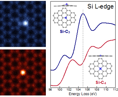
Fig. 2: Direct determination of the chemical bonding of single Si atoms via combination of ADF and spectrum imaging with first-principles calculations. (Left) ADF images of 3- and 4-fold coordinated Si atoms in graphene, and their respective Si L-edge fine structure extracted from spectrum images (Right). [3]. |