IT-9-O-1603 Split-Illumination Convergent Beam Electron Diffraction (SICBED) of Strained Crystals
Convergent beam electron diffraction (CBED) is a well-established Transmission Electron microscopy (TEM) method mainly used to characterize crystal structural properties like space group, charge density distribution or strain. CBED became very popular with the advent of stress engineering in microelectronics where the carriers mobility can be enhanced by tuning the strain of a channel in transistors. It is then of major interest to measure the strain state of the channel in order to understand the electronic properties of transistors. To tackle this problem, various strain measurement methods have been developed by X-Rays analysis, wafer curvature measurements or TEM techniques. Among different TEM methods (HREM, dark-field electron holography, (nano)diffraction, …) CBED is the most sensitive, because of the strong influence of the crystal parameters on the position of the High Order Laue Zone (HOLZ) lines. Furthermore, it has been shown by dynamical simulation method, that the HOLZ rocking curve is extremely sensitive to the displacement field changes along the electron beam path. This explains the occurrence of HOLZ line broadening when the strain is not constant along electrons trajectories in thin sample where surface relaxation occurs. CBED is therefore extremely efficient for local strain measurement, however, like all other strain measurement methods in TEM, the absolute strain measurements necessitates the use of an unstrained reference area. Depending on the sample geometry this reference can be located far from the area of interest. As example, in an epitaxial layer, due to stress relaxation, the substrate generally used as reference can be strained over hundreds of nanometers below the interface. In order to have access in a single CBED pattern to both the area where the strain measurement has to be performed and the unstrained reference (the latter being located microns apart from the former), we have developed a new convergent beam diffraction method, which combines split illumination and CBED optical configuration. This method called split-illumination CBED (Fig. 1) has been developed on the I2TEM microscope. I2TEM is an Hitachi HF3300C TEM fitted with a 300kV cold FEG, an electrostatic biprism located above the three condensors illumination system, two stages capability, a multibrism set-up, a 4k X 4k camera and a Cs-corrector from CEOS. The biprism located above the condenser system and the adjustment of the three condensors allow to separate the convergent beam in two parts which can be shifted apart on the surface of the sample and be recombined in the focal plane of the objective lens. In a single CBED disk, this allows half of the disk to from the strained region and half from a reference region located far from it (Fig. 2).
The authors acknowledge financial support from the European Union under the Seventh Framework Programme under a contract for an Integrated Infrastructure Initiative Reference 312483-ESTEEM2 and the National Research Agency under the program “Investissement d’Avenir” reference No. ANR-10-38-01-EQPX.
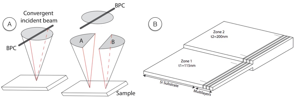
Fig. 1: A : SICBED optical configuration. The condenser biprism is used to split the beam convergent in two parallel half cones. B: Geometry of the FIB prepared SiGe/Si multilayers sample studied by SICBED |
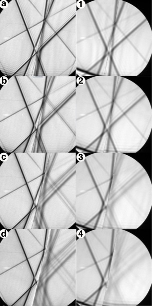
Fig. 2: SICBED patterns obtained when the condenser biprism voltage increase. Zone 2 (a=0V, b=3V, c=6V, d=9V), Zone 1 (1=0V, 2=3V, 3=6V, 4=9V) |