IT-9-P-1526 PRECESSED NANO-ELECTRON DIFFRACTION PATTERNS OF THE HUMAN TOOTH ENAMEL CRYSTALS
In this work we present the precessed electron diffraction patterns of the nano-sized human-tooth-enamel crystallites. These diffraction patterns have allowed us to obtain crystallography information the enamel’s unit cell [1].
The intensity of selected area electron diffraction (SAED) and nano-electron diffraction (n-ED) patterns is difficult to interpret due to the multiple interactions which take place (dynamical diffraction, absorption, etc). However, when the electron beam is tilted and precessed at high frequency the dynamic effect is minimized [2]. The crystal is not moving but the Ewald’s sphere is precessing around the optical axis producing that the dynamical SAED patterns become close to kinematical conditions and they can be used to obtain information on crystal structures [3, 4].
We have obtained the precessed n-ED from human tooth enamel crystals along different zone axes. Human tooth enamel is composed in 95% of hydroxyapatite crystals (HAP, Ca10(PO4)6(OH)2). These crystals are elongated-plate-like of 30 to 60 nm wide and 100 to 200 nm long [5], approximately (figure 1).
The human tooth enamel samples were obtained from permanent non-carious human molar teeth, extracted for orthodontic or periodontal reasons. Samples were prepared in the FIB-FEI QUANTA 200 3D equipment using the two beams system. A Philips CM30 transmission electron microscope with LaB6 filament working at 300 KV was used for TEM observation, the n-ED and the precessed electron diffraction patterns obtaining using a double-tilt holder. The precession of electron diffraction patterns were obtained with the Nanomegas “Spinning Star” equipment. The patterns were recorded on a Gatan “ORIUS” CCD camera using the Digital Micrograph software. JEMS software (version 3.8431U2012) was used for electron diffraction simulation.
Therefore, we have obtained precessed nano-electron diffraction patterns from crystals in the range from 30 to 100 nm (figure 2).
References
1. See papers in Ultramicroscopy, vol.107, issue 6-7, July 2007.
2. R. Vincent, P.A. Midgley, Ultramicroscopy 53 (1994) 271-282.
3. J.P. Morniroli, A. Redjaımia, S. Nicolopoulos, Ultramicroscopy 107 (2007) 514-522.
4. H. Klein Acta Cryst. A67, (2011) 303-309.
5. J. Reyes-Gasga et al., Materials Sci. Eng. C 33 (2013) 4568-4574.
JRG thanks to DGAPA-UNAM (contract IN106713), CONACYT and PASPA-DGAPA-UNAM for sabbatical support.
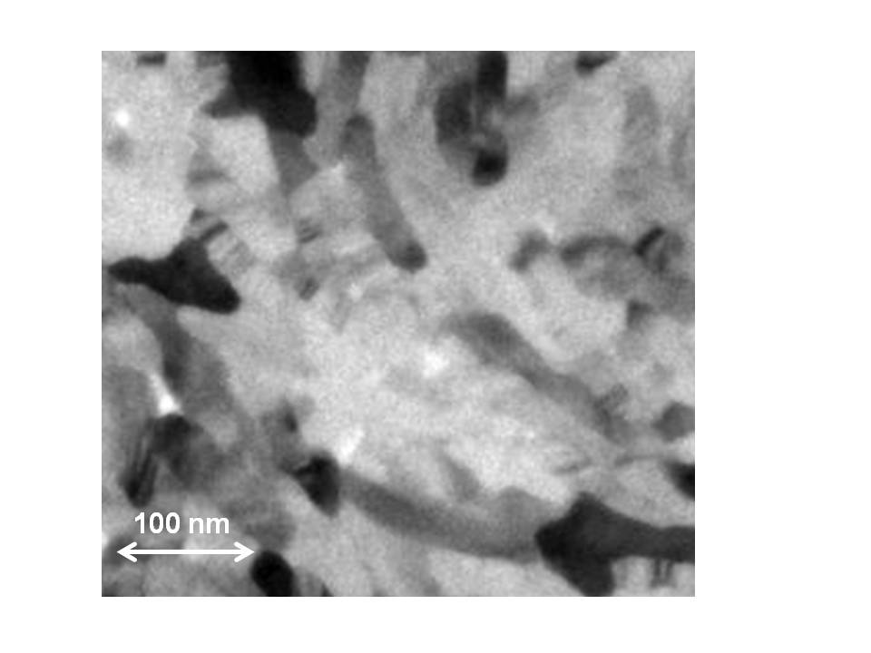
Fig. 1: TEM bright field image of the human tooth enamel FIB sample used in this work. Note the nano-sized crystals. |
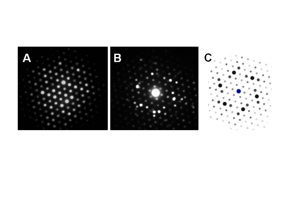
Fig. 2: Nano-electron diffraction pattern along the [0001] zone axis (A) and the corresponding precessed electron diffraction pattern (B). C) Simulated [0001] electron diffraction pattern for a HAP sample with thickness sample of 15 nm. |