IT-13-P-1517 Cross sectional sample preparation of nanowires for TEM analysis using FIB
Structuring of materials on the nanoscale is a common way to increase performance in a wide variety of devises. Nanostructures are a challenge for transmission electron microscopy (TEM) sample preparation, as they typically extend from the substrate without surrounding material. One solution has been to remove the nanostructures from their substrate and place them on a TEM grid. Although being simple and time efficient preparation method, it is not always adequate. If the nanostructure-substrate interface is of interest, the structures have a thickness of more than a few hundreds nm, or a TEM projection direction along a long axis is required, an alternative preparation method is necessary.
Here we report on methods for FIB sample preparation for TEM analysis of GaAs-GaInP core shell nanowires. By using polymer resin as support and protection we are able to produce cross-sections both perpendicular to and parallel with the substrate surface with minimal damage. Consequently nanowires grown perpendicular to the substrates could be imaged both in plan and side view, including the nanowire-substrate interface in the latter case. The nanowires, which are roughly 1.5 µm high and 350 nm in diameter, were grown on a GaAs substrate using metalorganic vapour phase epitaxy.
For plan view cross-section, the nanowires were first casted in a tablet-shaped mold using Spurr’s epoxy. The tablet was mechanically polished on one side until a section of the GaAs substrate was exposed. A TEM lamella was extracted using standard in-situ lift out method.
For side view cross-section, the nanowires were first covered in polymer resin by spin coating. Lithography resist proved to be a suitable resin as recipes for precise thickness are available from the resist manufacturers. The viscosity proved low enough not the bend the nanowires during spin coating. After spin coating the resin was soft baked on a hot plate, which increased the viscosity without affecting the nanowires. Finally, a TEM lamella was extracted using standard in-situ lift out method.
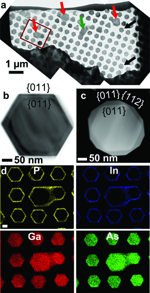
Fig. 1: a) TEM overview of plan view cross-section lamella. b) TEM image of upper nanowire marked with a black arrow in a). Shell and core have {011} facets. c) STEM HAADF image of lower nanowire cross-sections marked with a black arrow in a). The shell have both {011} and {112} facets. d) STEM XEDS maps from the red rectangle in a) (scale bar is 100 nm). |
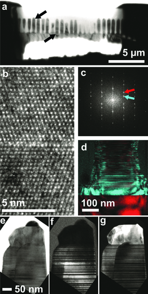
Fig. 2: a) TEM overview of side view cross-section lamella. b) HRTEM image of interface marked in a). c) diffractogram of image b). d) DFTEM images, colors correspond to diffractions spots marked in c). e) TEM image from tip of nanowire marked in a). f) DFTEM image from a wurtzite diffraction spot. g) DFTEM image from a zincblende diffraction spot. |