IT-4-P-1503 Using an EBSD Detector as a Microstructural Imaging Device
Electron Backscatter Diffraction (EBSD) has proven to be a useful tool for characterizing the crystallographic orientation aspects of microstructures at length scales ranging from tens of nanometers to millimetres in the the scanning electron microscope (SEM). With the advent of high-speed digital cameras for EBSD use, it has become practical to the EBSD detector as an imaging device similar to a backscatter (or forward-scatter) detector [1-3]. When the EBSD detector is used in this manner, images exhibiting topographic, atomic density and orientation contrast can be obtained at rates similar to slow scanning in the conventional SEM manner. The same high-tilt (~70°) sample geometry is used and the camera is binned considerably – to a 5x5 “super-pixel” image - in order to get extremely fast acquisition rates. At such high binning, the captured patterns are not suitable for indexing. However, no indexing is required to for using the detector as an imaging device. Rather, a 5x5 array of images is formed by essentially using each super-pixel as an individual scattered electron detector as shown in Figure 1. The images formed in this way can then be combined in a variety of ways to form composite images of the microstructure as shown in Figure 2. The flexibility to combine these images together allows different contrast mechanisms to be emphasized in the composite images. While images formed in this manner lack the quantitative nature of the maps formed by using EBSD in the traditional manner, they still provide a wealth of information that can be obtained at rates much faster than the quantitative EBSD maps and with much less EBSD expertise required by the operator.
References
[1] S. I. Wright & M. M. Nowell (2006) “Microstructure Characterization Using EBSD Image Quality Mapping”, Presentation at THERMEC, Vancouver, Canada.
[2] R. Schwarzer, J. Sukkau & J. Hjelen (2011) “Imaging of topography and phase distributions with an EBSD detector in the SEM”, Poster presentation at Microscopy Conference, Kiel, Germany.
[3] E. J. Payton, L. Agudo Jácome & G. Nolze (2013) “Phase Identification by Image Processing of EBSD Patterns” Presentation at Microscopy & Microanalysis, Indianapolis, USA.
Scott Lindeman of EDAX is gratefully acknowledged for his assitance.
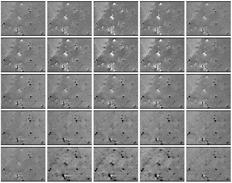
Fig. 1: A five by five array of images formed using a heavily binned EBSD detector as an array of twenty-five individual scattered electron detectors from a Mylonite sample. |
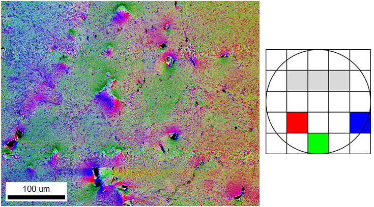
Fig. 2: A composite image formed by combining the individual images shown in Figure 1together in the manner shown in the accompanying schematic. The circular outline in the schematic shows the position of the phosphor screen relative to the 5x5 pixel array. |