IT-4-P-1467 Energy Low Loss Backscattered Electrons Imaging in Material Characterization and Analysis
With the continuous size and structure shrinkage in semiconductor and electronic devices, the final performance and properties of the materials are dominated by the surface and interface layers. This requires scanning electron microscope (SEM) as a most conventional technical method in material characterization and analysis not only to be able to visualize and image such nanostructures with the secondary electron imaging under a low energy beam but also to analyze the tiny compositional differences like doping contrast, oxidation states of elements, small phases of hybrids or function group in polymers etc., which are not available via the classical backscattered electron imaging or other Energy-dispersive X-ray spectroscopy methods. Although the classical backscattered electron (BSE) imaging are from the multiple inelastic scattering process which could provide density related contrast like channeling contrast at high energy beam, the backscattering coefficient shows non-linear behavior and get very complicated.
In the classical backscattering process (Rutherford scattering), the backscattered electrons are mainly from the scattering of the high energy primary electrons with the nucleus charge or inner electron shells of the material. In such a case the contrast or brightness of the BSE imaging scale with material density, atomic number (Z). However the scattering between the primary beam with the outer electron shells of the materials at low impact energy (below 3 kV) region is not any more negligible which even becomes more dominant where the surface plasma resonance and ionization loss could happen and contribute to in the total contrast mechanism.
The unique design of the Gemini® lens integrated with a beam booster in the beam path not only maintains the brightness of the downward primary electron beam at low energies but also has a dispersion function for the generated reverse electron signals backward into the column. It means that the secondary electrons and backscattered electrons with a small energy and angle differences could be amplified and separated by the Gemini® lens in real time and space without converting the signals or by applying any additional stage bias. The separated backscattered electrons could be further filtered with an energy filtering grid and projected back into the corresponding detector. Backscattered electrons with a specific energy low loss could be picked out for imaging by setting an appropriate threshold potential to the filtering grid. After the grid filter the multiple inelastic scattered electrons could be cut away and the signal is consisted of the so-called energy low loss backscattered electrons which reveals some characteristic resonance of the materials.
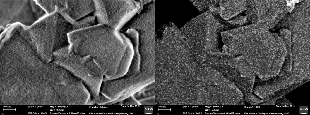
Fig. 1: The SE1 image (left) and corresponding LL-BSE image (right) of the Ceincorporated into mesoporous silica as catalyst where the Ce ions andnanoclusters give high brightness. |
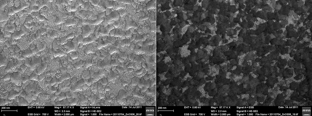
Fig. 2: The SE1 image (left) and corresponding LL-BSE image (right) of the ZnSxO1-x thin film on Al2O3 substrate where the LL-BSE image is from the low loss BSEs with an energy between 700 eV and 800 eV. |